M5M5W816WG 查看數據表(PDF) - Renesas Electronics
零件编号
产品描述 (功能)
生产厂家
M5M5W816WG Datasheet PDF : 10 Pages
| |||
2002.04.18 Ver. 6.0
M5M5W816WG - 55HI, 70HI, 85HI
MITSUBISHI LSIs
8388608-BIT (524288-WORD BY 16-BIT) CMOS STATIC RAM
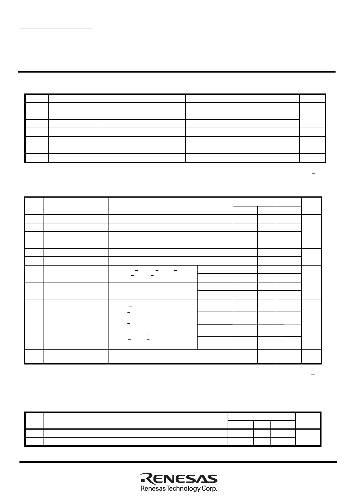
ABSOLUTE MAXIMUM RATINGS
Symbol
Parameter
Vcc Supply v oltage
VI
Input v oltage
VO Output v oltage
Pd Power dissipation
Ta
Operating
temperature
T stg Storage temperature
Conditions
With respect to GND
With respect to GND
With respect to GND
Ta= 25°C
Ratings
-0.3* ~ +4.6
-0.3* ~ Vcc + 0.3 (max. 4.6V)
0 ~ Vcc
700
Units
V
mW
- 40 ~ +85
°C
- 65 ~ +150
°C
* -3.0V in case of AC (Pulse width < 30ns)
DC ELECTRICAL CHARACTERISTICS
( Vcc=2.7 ~ 3.6V, unless otherwise noted)
Symbol
Parameter
Conditions
VIH High-lev el input v oltage
VIL Low-lev el input v oltage
VOH High-lev el output v oltage IOH= -0.5mA
VOL Low-lev el output v oltage IOL=2mA
II Input leakage current
VI =0 ~ Vcc
IO Output leakage current BC1# and BC2# =VIH or S1# =VIH or S2=VIL or OE# =VIH, VI/O=0 ~ Vcc
Icc1 Activ e supply c urrent
( AC,MOS lev el )
BC1# and BC2# < 0.2V, S1# < 0.2V, S2 > Vcc-0.2V
other inputs < 0.2V or > Vcc-0.2V
Output - open (duty 100%)
f = 10MHz
f = 1MHz
Activ e supply c urrent
Icc2
( AC,TTL lev el )
BC1# and BC2#=V IL , S1#=V IL ,S2=V IH
other pins =V IH or VIL
Output - open (duty 100%)
f = 10MHz
f = 1MHz
Icc3 Stand by s upply current
( AC,MOS lev el )
(1) S1# > Vcc - 0.2V,
S2 > Vcc - 0.2V,
other inputs = 0 ~ Vcc
(2) S2 < 0.2V,
other inputs = 0 ~ Vcc
(3) BC1# and BC2# > Vcc - 0.2V
S1# < 0.2V, S2 > Vcc - 0.2V
other inputs = 0 ~ Vcc
~ +25°C
~ +40°C
~ +70°C
~ +85°C
Stand by s upply current BC1# and BC2# =VIH or S1# =VIH or S2 =VIL
Icc4
( AC,TTL lev el ) Other inputs= 0 ~ Vcc
Min
2.2
-0.2 *
2.4
-
-
-
-
-
-
-
-
-
Limits
Ty p
Max Units
Vcc+0.2V
0.6
V
0.4
±1
µA
±1
30 50
5
15
30 50
mA
5
15
0.5 5
1.0 8
µA
-
20
-
40
-
2 mA
Note 1: Direction for current flowing into IC is indicated as positive (no mark).
* -1.0V in case of AC (Pulse width < 30ns)
Note 2: Typical parameter indicates the value for the center of distribution at 3.0V, and is not 100% tested.
CAPACITANCE
Symbol Parameter
CI
Input capacitance
CO Output capacitance
Conditions
VI=GND, VI=25mVrms, f =1MHz
VO=GND,VO=25mVrms, f =1MHz
(Vcc=2.7 ~ 3.6V, unless otherwise noted)
Limits
Min Ty p Max
10
10
Units
pF
3
Share Link: 