M5M5V416BRT 查看數據表(PDF) - Renesas Electronics
零件编号
产品描述 (功能)
生产厂家
M5M5V416BRT Datasheet PDF : 10 Pages
| |||
revision-P11, ' 03.01.14
M5M5V416BTP,RT
MITSUBISHI LSIs
AC ELECTRICAL CHARACTERISTICS
(1) TEST CONDITIONS
4194304-BIT (262144-WORD BY 16-BIT) CMOS STATIC RAM
(Vcc=2.7 ~ 3.6V, unless otherwise noted)
Supply v oltage
2.7V~3.6V
Input pulse
V IH= 2 . 4 V , V IL= 0 . 4 V
Input rise time and f all time 5ns
Ref erence lev el
Output loads
(2) READ CYCLE
V OH=V OL= 1 . 5 V
Transition is measured ±500mV f rom
steady state voltage.(f or ten,t dis)
Fig.1,CL=30pF
CL=5pF (for ten,tdis)
Limits
Symbol
Parameter
t CR
ta(A)
ta(S1)
ta(S2)
ta(BC1)
ta(BC2)
ta(OE)
tdis(S1)
tdis(S2)
tdis(BC1)
tdis(BC2)
tdis(OE)
ten(S1)
ten(S2)
ten(BC1)
ten(BC2)
ten(OE)
tV(A)
Read cy cle time
Address access time
Chip select 1 access time
Chip select 2 access time
By te control 1 access time
By te control 2 access time
Output enable access time
Output disable time af t er S1 high
Output disable time af t er S2 low
Output disable time af t er BC1 high
Output disable time af t er BC2 high
Output disable time af t er OE high
Output enable time af ter S1 low
Output enable time af ter S2 high
Output enable time af ter BC1 low
Output enable time af ter BC2 low
Output enable time af ter OE low
Data v alid time after address
(3) WRITE CYCLE
Min
70
10
10
10
10
5
10
Limits
Symbol
Parameter
Min
tCW
Write cy cle time
70
tw(W)
Write pulse width
55
tsu(A)
Address setup time
0
tsu(A-WH) Address setup time with respect to W
60
tsu(BC1) By te control 1 setup time
60
tsu(BC2) By te control 2 setup time
60
tsu(S1) Chip select 1 setup time
60
tsu(S2) Chip select 2 setup time
60
tsu(D)
Data setup time
35
th(D)
Data hold time
0
trec(W) Write recov ery time
0
tdis(W) Output disable time f rom W low
tdis(OE) Output disable time f rom OE high
ten(W) Output enable time f rom W high
5
ten(OE) Output enable time f rom OE low
5
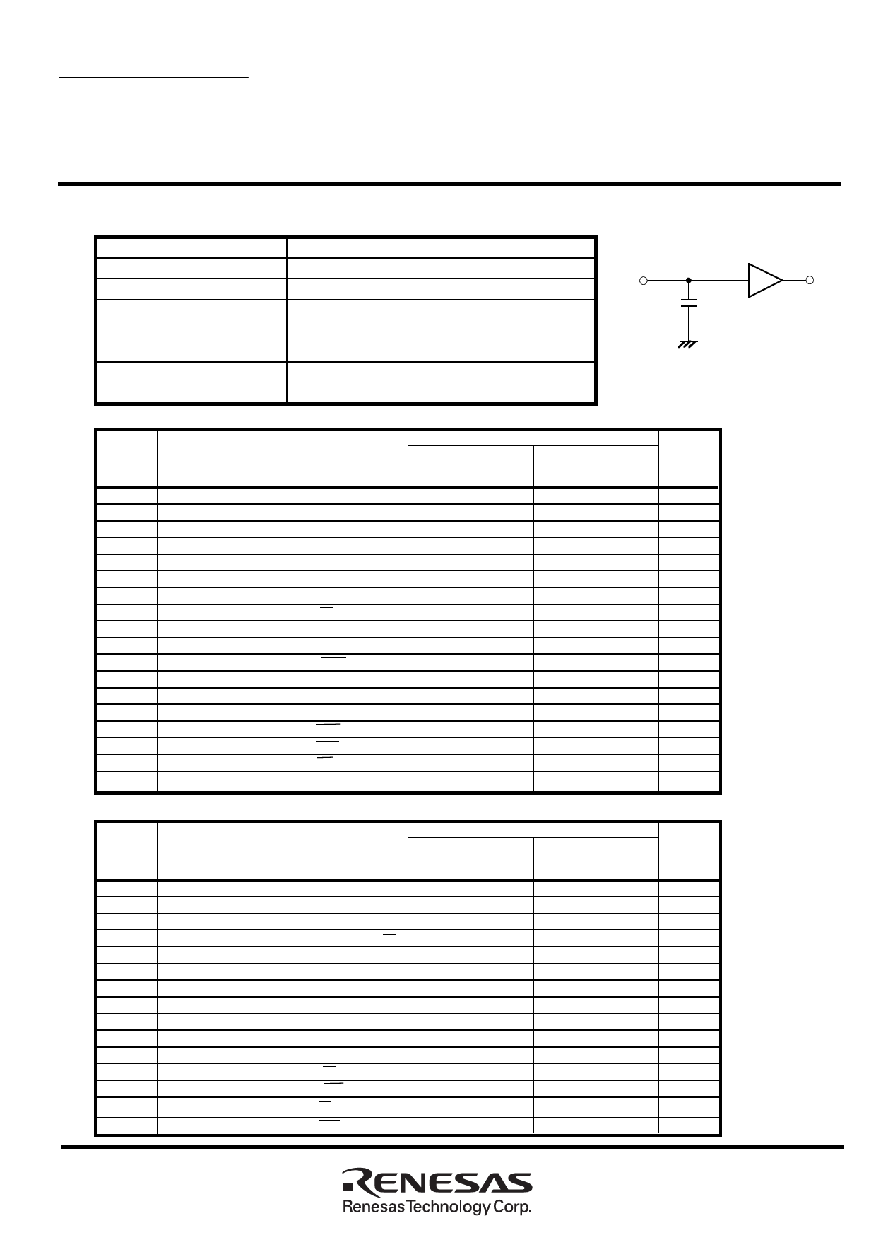
DQ
Max
70
70
70
70
70
35
25
25
25
25
25
Max
25
25
1TTL
CL
Including scope and
jig capacitance
Fig.1 Output load
Units
ns
ns
ns
ns
ns
ns
ns
ns
ns
ns
ns
ns
ns
ns
ns
ns
ns
ns
Units
ns
ns
ns
ns
ns
ns
ns
ns
ns
ns
ns
ns
ns
ns
ns
4
Share Link: 