M62500P 查看數據表(PDF) - Mitsumi
零件编号
产品描述 (功能)
生产厂家
M62500P Datasheet PDF : 11 Pages
| |||
MITSUBISHI (Dig./Ana. INTERFACE)
M62500P/FP
SYNCHRONIZATION DEFLECTION SYSTEM CONTROL PWM IC
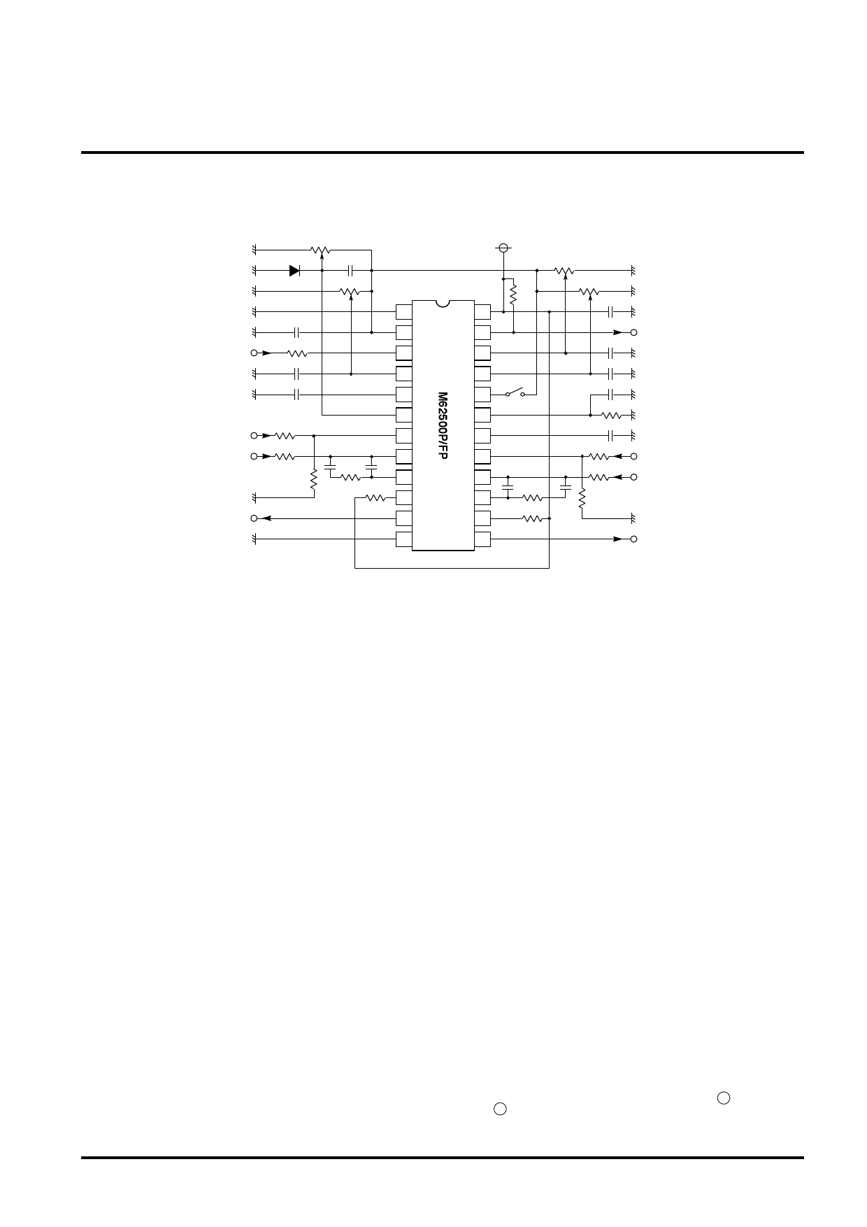
APPLICATION EXAMPLE
Tin
+IN1
-IN1
OUT1
VR2
D1
C4
VR1
C1
R1
C2
Cagc1
R2
R4
R3
C4
R5
1
2
3
4
5
6
7
8
C3
9
R6
10
11
12
VCC
24
R12
23
22
21
20
19
18
17
16
R9
15 C5 R7
14
13
VR4
VR3
C10
DOUT
C9
C8
C7
Ragc
Cagc2
R10
+IN2
-IN2
R8
C6 R11
OUT2
C1, C10
VR 1, 2, 3, 4
C2, C8, C9
C4, D1
R1
Cagc 1, 2
: Is required for stabilization of Vcc and VREF.
Is normally set to tens of µF to hundreds of
µF.
: Is determined taking into account the load
capability of VREF. (External load capability
of approx. 5mA) Shall be normally set to
approx. 10kΩ.
: Is added to high impedance pin of voltage
control for improvement in noise margin.
Depends on the device installation
environment. Shall be normally set to approx.
0.1µF.
: Is added for the execution of software start.
Set a time constant, taking into account the
set value of VR2.
: Is added to reduce interference by Tin and
outputs. With VIN=approx. 2.5V to 5V, the
resistance value of approx. 22kΩ is
recommended.
: Capacitance necessary for stabilization of
AGC. As the capacitance is larger, the
stability is larger, but the characteristic of
answering becomes worse. The capacitance
value of 1µF is recommended.
R2, R3, R10, R11 : A gain setup constant of error Amp. To
R4, R5, R8, R9
assure the stability of feedback, R4 and R8
C3, C4, C5, C6
shall be set to several kΩ to tens of kΩ to set
the gain to approx. 20dB to 40dB with f=1
kHz. If the gain is too low, jitter may take
place. It is therefore recommended to set C3
and C5 to tens of pF to hundreds of pF, C4
and C6 to thousands of pF to tens of
thousands of pF, and R5 and R9 to tens of
kΩ to hundreds of kΩ.
Ragc
: Resistance for setting AGC on the OUT2
side. Is set with Ragc=27kΩ.
C7
: If f to be input into Tin suddenly changes,
addition of C7 shortens non-control time of
Dout (output of "H"). As a capacitance value,
it is recommended to adopt 2.2µF. In the
case of adding C7, however,
Cagc2≥0.68µF is recommended.
R6, R7
: Current limit resistance of OUT1/2. Is
normally set to several Ω. Insertion of direct
limit resistance into OUT1/2 pin is also
effective.
R12
: Pull-up resistance of DOUT output. DOUT is
an open collector output and requires R12. Is
normally set to several kΩ.
* Note: To reduce interference in the signal system, pins 1 GND and
12 P.GND shall be grounded at a point in the power supply block.
( 7 / 11 )
Share Link: 