AS7C31024-10JC жҹҘзңӢж•ёж“ҡиЎЁпјҲPDFпјү - Alliance Semiconductor
йӣ¶д»¶зј–еҸ·
дә§е“ҒжҸҸиҝ° (еҠҹиғҪ)
з”ҹдә§еҺӮ家
AS7C31024-10JC Datasheet PDF : 9 Pages
| |||
AS7C1024
AS7C31024
В®
Functional description
The AS7C1024 and AS7C31024 are high performance CMOS 1,048,576-bit Static Random Access Memory (SRAM) devices
organized as 131,072 words Г— 8 bits. It is designed for memory applications where fast data access, low power, and simple
interfacing are desired.
Equal address access and cycle times (tAA, tRC, tWC) of 10/12/15/20 ns with output enable access times (tOE) of 5/6/8/10 ns
are ideal for high performance applications. Active high and low chip enables (CE1, CE2) permit easy memory expansion with
multiple-bank systems.
When CE1 is high or CE2 is low the devices enter standby mode. If inputs are still toggling, the device will consume ISB power.
If the bus is static, then full standby power is reached (ISB1 or ISB2). For example, the AS7C31024 is guaranteed not to exceed
0.33mW under nominal full standby conditions. All devices in this family will retain data when VCC is reduced as low as 2.0V.
A write cycle is accomplished by asserting write enable (WE) and both chip enables (CE1, CE2). Data on the input pins I/O0-
I/O7 is written on the rising edge of WE (write cycle 1) or the active-to-inactive edge of CE1 or CE2 (write cycle 2). To avoid
bus contention, external devices should drive I/O pins only after outputs have been disabled with output enable ( OE) or write
enable (WE).
A read cycle is accomplished by asserting output enable (OE) and both chip enables (CE1, CE2), with write enable (WE) high.
The chips drive I/O pins with the data word referenced by the input address. When either chip enable is inactive, output
enable is inactive, or write enable is active, output drivers stay in high-impedance mode.
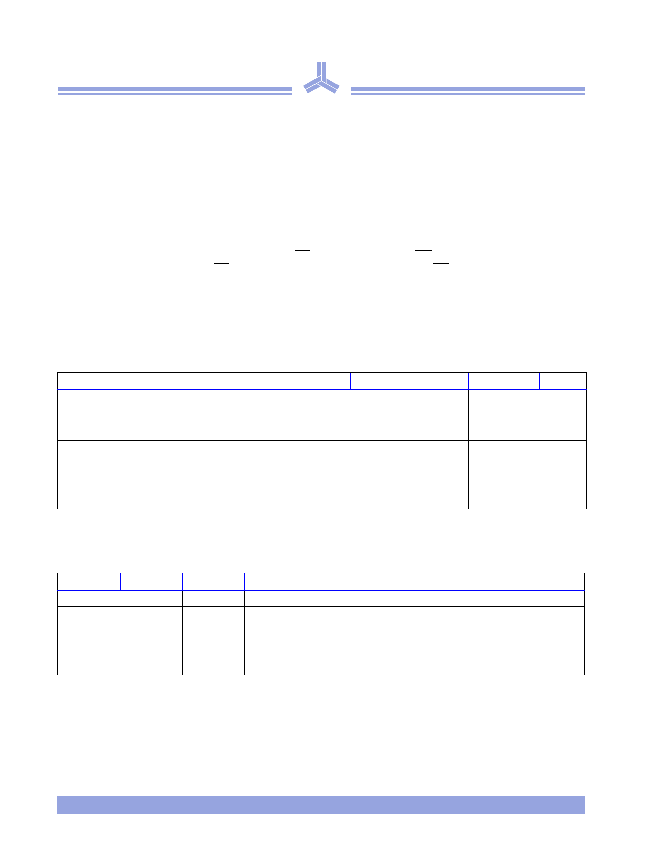
Absolute maximum ratings
Parameter
Symbol
Min
Max
Unit
Voltage on VCC relative to GND
Voltage on any pin relative to GND
Power dissipation
Storage temperature (plastic)
Ambient temperature with VCC applied
DC current into outputs (low)
AS7C1024
AS7C31024
Vt1
Vt1
Vt2
PD
Tstg
Tbias
IOUT
вҖ“0.50
-0.50
вҖ“0.50
вҖ“
вҖ“65
вҖ“55
вҖ“
+7.0
V
+5.0
V
VCC +0.50
V
1.0
W
+150
В°C
+125
В°C
20
mA
Note: Stresses greater than those listed under Absolute Maximum Ratings may cause permanent damage to the device. This is a stress rating only and functional
operation of the device at these or any other conditions outside those indicated in the operational sections of this specificati on is not implied. Exposure to
absolute maximum rating conditions for extended periods may affect reliability.
Truth table
CE1
CE2
WE
OE
H
X
X
X
X
L
X
X
L
H
H
H
L
H
H
L
L
H
L
X
Key: X = DonвҖҷt Care, L = Low, H = High
Data
High Z
High Z
High Z
DOUT
DIN
Mode
Standby (ISB, ISB1)
Standby (ISB, ISB1)
Output disable (ICC)
Read (ICC)
Write (ICC)
2
ALLIANCE SEMICONDUCTOR
11/29/00
Share Link: 