MAX17000 查看數據表(PDF) - Maxim Integrated
零件编号
产品描述 (功能)
生产厂家
MAX17000 Datasheet PDF : 32 Pages
| |||

MAX17000
Complete DDR2 and DDR3 Memory
Power-Management Solution
ABSOLUTE MAXIMUM RATINGS
TON to PGND1 .......................................................-0.3V to +28V
VDD to PGND1..........................................................-0.3V to +6V
VCC to VDD ............................................................-0.3V to +0.3V
OVP to AGND ...........................................................-0.3V to +6V
SHDN, STDBY, SKIP to AGND .................................-0.3V to +6V
REFIN, FB, PGOOD1,
PGOOD2 to AGND ................................-0.3V to (VCC + 0.3V)
CSH, CSL to AGND ....................................-0.3V to (VCC + 0.3V)
DL to PGND1..............................................-0.3V to (VDD + 0.3V)
BST to PGND1...........................................................-1V to +34V
BST to LX..................................................................-0.3V to +6V
DH to LX ....................................................-0.3V to (VBST + 0.3V)
BST to VDD .............................................................-0.3V to +28V
VTTI to PGND2 .........................................................-0.3V to +6V
VTT to PGND2 ............................................-0.3V to (VTTI + 0.3V)
VTTS to AGND............................................-0.3V to (VCC + 0.3V)
VTTR to AGND ..........................................-0.3V to (VCSL + 0.3V)
PGND1, PGND2 to AGND.....................................-0.3V to +0.3V
Continuous Power Dissipation (TA = +70°C)
24-Pin, 4mm x 4mm TQFN-EP
(derated 27.8mW/°C above +70°C) ..........................2222mW
Operating Temperature Range ...........................-40°C to +85°C
Junction Temperature ......................................................+150°C
Storage Temperature Range .............................-65°C to +150°C
Lead Temperature (soldering, 10s) .................................+300°C
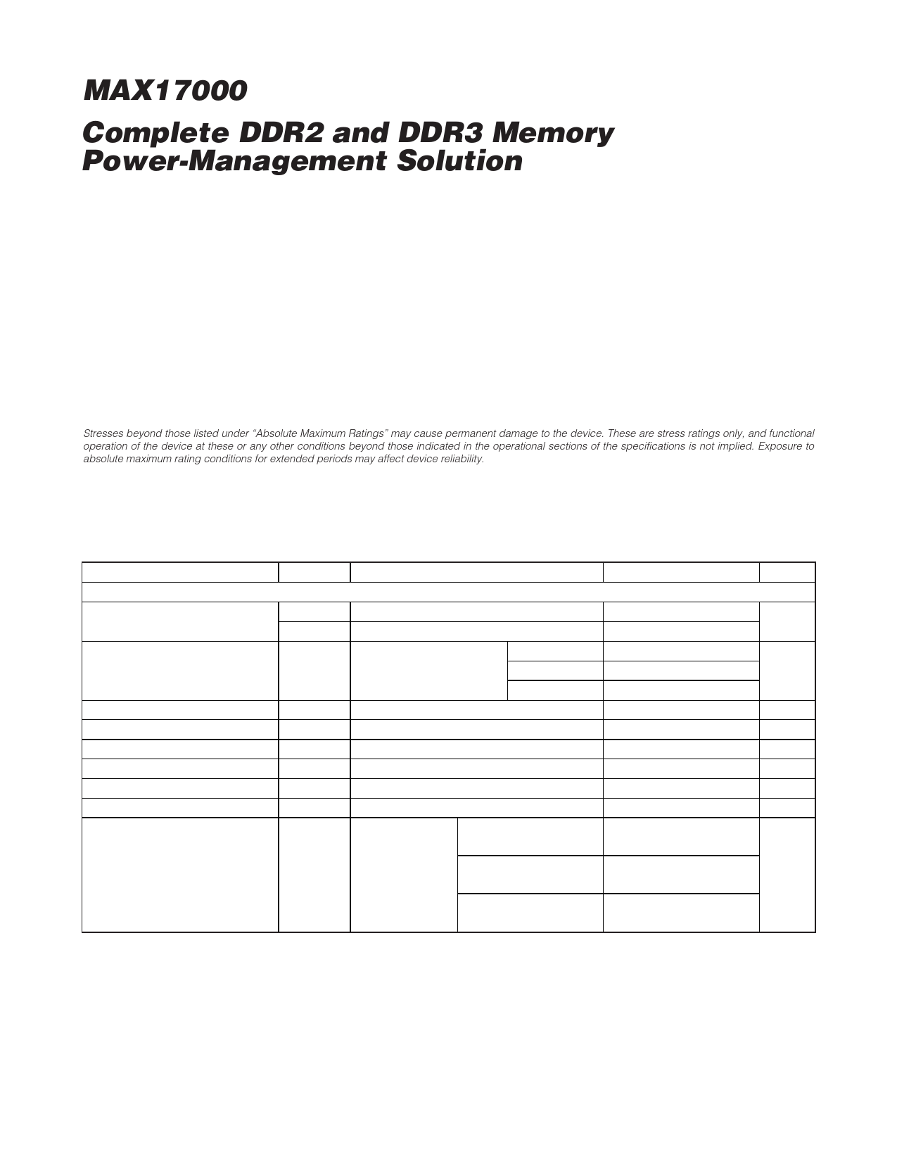
Stresses beyond those listed under “Absolute Maximum Ratings” may cause permanent damage to the device. These are stress ratings only, and functional
operation of the device at these or any other conditions beyond those indicated in the operational sections of the specifications is not implied. Exposure to
absolute maximum rating conditions for extended periods may affect device reliability.
ELECTRICAL CHARACTERISTICS
(VIN = 12V, VCC = VDD = VSHDN = VREFIN = 5V, VCSL = 1.8V, STDBY = SKIP = AGND, TA = 0°C to +85°C, unless otherwise noted.
Typical values are at TA = +25°C.) (Note 1)
PARAMETER
SYMBOL
CONDITIONS
MIN TYP MAX UNITS
PWM CONTROLLER
Input Voltage Range
Output Voltage Accuracy
VIN
VCC, VDD
VCSL
VIN = 4.5V to 26V,
SKIP = VCC
3
26
V
4.5
5.5
FB = AGND
1.485 1.500 1.515
FB = VCC
1.782 1.800 1.818
V
FB = Adj
0.99 1.000 1.01
Output Voltage Range
Load Regulation Error
Line Regulation Error
Soft-Start Ramp Time
Soft-Stop Ramp Time
Soft-Stop Threshold
VCSL
tSSTART
tSSTOP
VCSH - VCSL = 0 to 18mV, SKIP = VCC
VDD = 4.5V to 5.5V, VIN = 4.5V to 26V
Rising edge of SHDN
Falling edge of SHDN
1
2.7
V
0.1
%
0.25
%
1.4
2.1
ms
2.8
ms
25
mV
RTON = 96.75k
(600kHz), 167ns nominal
-15
+15
On-Time Accuracy (Note 2)
tON
VIN = 12V,
VCSL = 1.2V
RTON = 200k (300kHz),
333ns nominal
-10
+10
%
RTON = 303.25k
(200kHz), 500ns nominal
-15
+15
2
Maxim Integrated