MAX1741 жҹҘзңӢж•ёж“ҡиЎЁпјҲPDFпјү - Maxim Integrated
йӣ¶д»¶зј–еҸ·
дә§е“ҒжҸҸиҝ° (еҠҹиғҪ)
з”ҹдә§еҺӮ家
MAX1741 Datasheet PDF : 12 Pages
| |||
SIM/Smart Card Level Translators
in ВөMAX
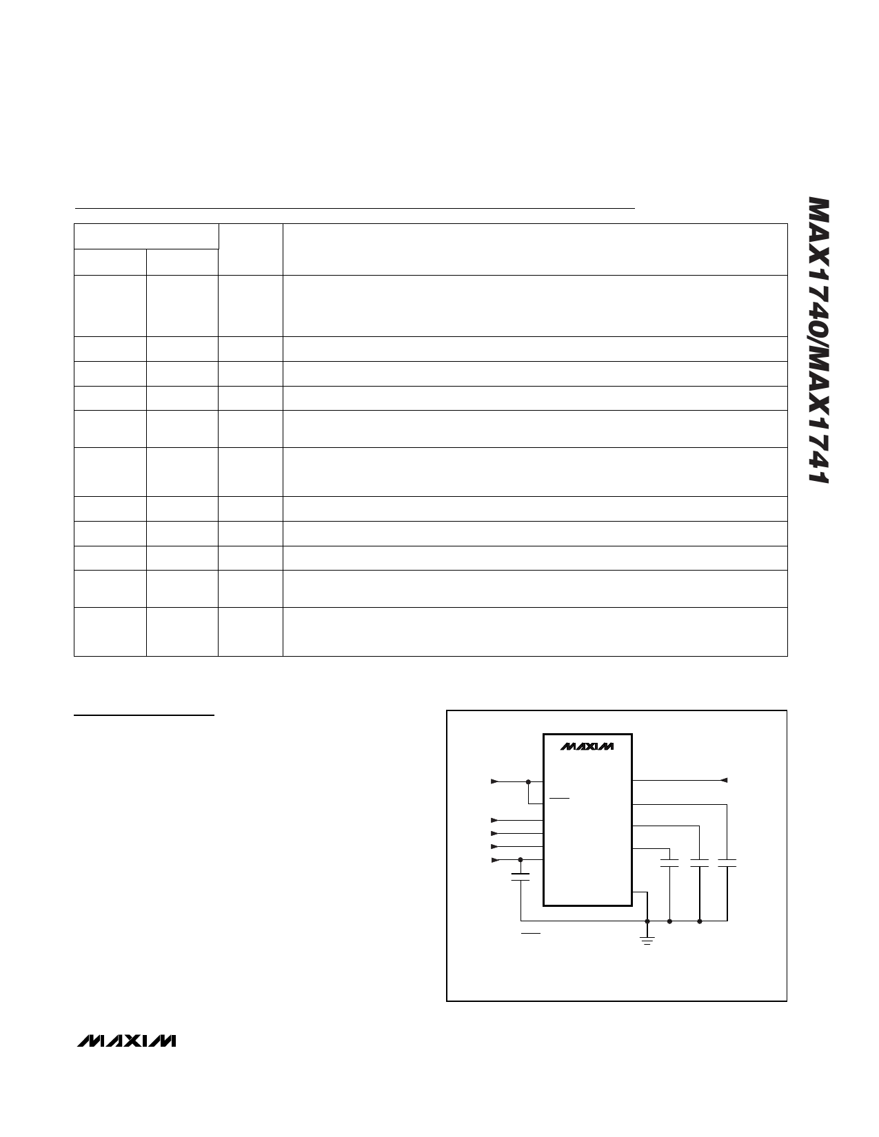
PIN
MAX1740 MAX1741
NAME
1
1
DATA
2
2
DVCC
3
3
CIN
4
4
RIN
вҖ”
5
DDRV
5
вҖ”
SHDN
6
6
GND
7
7
RST
8
8
CLK
9
9
VCC
10
10
IO
Pin Description
FUNCTION
System Controller Data Input/Output. An open-drain input/output with a 20kв„Ұ pull-up
resistor to DVCC. For bidirectional data transfer, connect to an open-drain controller output
capable of sinking 1mA while pulling DATA low. If the controller is not open drain, use
DDRV to send data and DATA to receive data.
Supply Voltage for System Controller Digital Pins. Set at +1.425V to +5.5V.
System Controller Clock Input
System Controller Reset Input
Optional System Controller Data Input. Connect to controllers without an open-drain out-
put. When not used, connect DDRV to DVCC.
Shutdown Mode Input. Driving SHDN low reduces the total supply current to less than
2ВөA. In shutdown mode, RST, CLK, and IO are actively pulled low and the transfer gate
between DATA and IO is disabled. When not used, connect SHDN to DVCC.
System Controller and Card Ground
Reset Output to Card. Actively pulled low during shutdown.
Clock Output to Card. Actively pulled low during shutdown.
Supply Voltage for Card-Side Digital Pins. Set at +2.25V to +5.5V. Proper supply bypass-
ing is required to meet Вұ10kV ESD specifications.
Card-Side Bidirectional Input/Output. An open-drain output with a 10kв„Ұ pull-up resistor to
VCC. For bidirectional data transfer, connect to an open-drain card output capable of sink-
ing 1mA while pulling IO low. Actively pulled low during shutdown.
Detailed Description
The MAX1740/MAX1741 provide the necessary level
translation for interfacing with subscriber identity mod-
ules (SIMs) and smart cards in multivoltage systems.
These devices operate with logic supply voltages
between +1.425V and +5.5V on the controller side
(DVCC) and between +2.25V and +5.5V on the card side
(VCC). The total supply current (IDVCC + IVCC) is 2.5ВөA
(max) while operating in an idle state (see Electrical
Characteristics). Figure 2 shows a typical application cir-
cuit and functional diagram.
Level Translation
The MAX1740/MAX1741 provide level translators for a
clock input, a reset input, and a bidirectional data
input/output. The clock and reset inputs (CIN and RIN)
are level shifted from the controller-side supply rails
(DVCC to GND) to the card-side supply rails (VCC to
GND). When connected to an open-drain controller out-
put, DATA and IO provide bidirectional level translation.
+1.8V
30pF
MAX1740
MAX1741
DVCC
VCC
SHDN*
RST
RIN
CLK
CIN
DDRV*
IO
DATA
GND
+3.0V OR
+5.0V
30pF 30pF 30pF
* SHDN FOR MAX1740 ONLY
DDRV FOR MAX1741 ONLY
NOTE: ALL CAPACITANCES INCLUDE CAPACITIVE LOADS OF
TEST PROBES AND BOARD LAYOUT.
Figure 1. MAX1740/MAX1741 Test Circuit
_______________________________________________________________________________________ 7
Share Link: 