LC75811W 查看數據表(PDF) - SANYO -> Panasonic
零件编号
产品描述 (功能)
生产厂家
LC75811W Datasheet PDF : 27 Pages
| |||
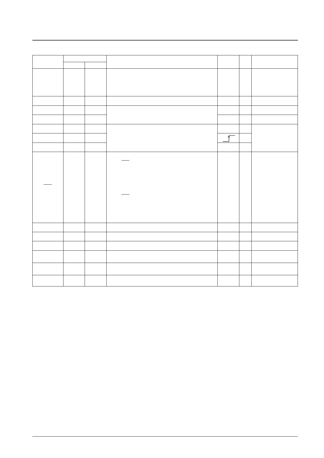
LC75811E, 75811W
Pin Functions
Pin
S1 to S58
S59/COM10
S60/COM9
Pin No.
LC75811E LC75811W
Function
1 to 58
59
60
79, 80
1 to 56
57
58
Segment driver outputs.
The S59/COM10 and S60/COM9 pins can be used as common
driver outputs under the “set display technique” instruction.
COM1 to COM8 68 to 61 66 to 59 Common driver outputs.
OSCI
OSCO
CE
CL
DI
76
74
Oscillator connections. An oscillator circuit is formed by
75
73
connecting an external resistor and capacitor at these pins.
78
76
Serial data transfer inputs. These pins are connected to the
microcontroller.
79
77
CE: Chip enable
CL: Synchronization clock
80
78
DI: Transfer data
Active
—
—
—
—
H
—
RES
Reset signal input.
• When RES is low (VSS):
• Display off
S1 to S58 = “L” (VSS).
S59/COM10 and S60/COM9 = “L” (VSS).
COM1 to COM8 = “L” (VSS).
77
75
• Serial data transfer is disabled.
L
• The OSCI/OSCO pin oscillator is stopped.
• When RES is high (VDD):
• Display on after a “display on/off control” (display on
state setting) instruction is executed.
• Serial data transfers are enabled.
• The OSCI/OSCO pin oscillator operates.
VLCD1
VLCD2
VLCD3
VDD
VLCD
VSS
71
69
Used for applying the LCD drive 3/4 bias voltage externally.
—
72
70
Used for applying the LCD drive 2/4 bias voltage externally.
—
73
71
Used for applying the LCD drive 1/4 bias voltage externally.
—
69
67
Logic block power supply connection. Provide a voltage of
between 2.7 and 6.0 V.
—
70
68
LCD driver block power supply connection. Provide a voltage of
between 4.5 and 10.0 V.
—
74
72
Power supply connection. Connect to ground.
—
I/O Handling when unused
O
OPEN
O
OPEN
I
GND
O
OPEN
I
I
GND
I
I
GND
I
OPEN
I
OPEN
I
OPEN
—
—
—
—
—
—
No. 5915-6/27
Share Link: 