MAX4411BEBE-T 查看數據表(PDF) - Maxim Integrated
零件编号
产品描述 (功能)
生产厂家
MAX4411BEBE-T
Maxim Integrated

MAX4411BEBE-T Datasheet PDF : 18 Pages
| |||
80mW, Fixed-Gain, DirectDrive, Stereo
Headphone Amplifier with Shutdown
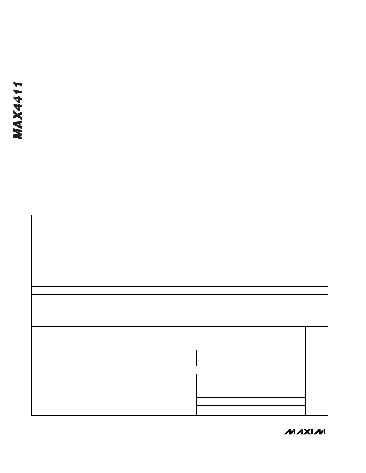
ABSOLUTE MAXIMUM RATINGS
PGND to SGND .....................................................-0.3V to +0.3V
PVDD to SVDD .................................................................-0.3V to +0.3V
PVSS to SVSS .........................................................-0.3V to +0.3V
PVDD and SVDD to PGND or SGND .........................-0.3V to +4V
PVSS and SVSS to PGND or SGND ..........................-4V to +0.3V
IN_ to SGND ................................(SVSS - 0.3V) to (SVDD + 0.3V)
SHDN_ to SGND........................(SGND - 0.3V) to (SVDD + 0.3V)
OUT_ to SGND .............................(SVSS - 0.3V) to (SVDD +0.3V)
C1P to PGND.............................(PGND - 0.3V) to (PVDD + 0.3V)
C1N to PGND .............................(PVSS - 0.3V) to (PGND + 0.3V)
Output Short Circuit to GND or VDD...........................Continuous
Continuous Power Dissipation (TA = +70°C)
16-Bump UCSP (derate 7.4mW/°C above +70°C)........589mW
20-Pin Thin QFN (derate 16.9mW/°C above +70°C) ..1349mW
Junction Temperature ......................................................+150°C
Operating Temperature Range ...........................-40°C to +85°C
Storage Temperature Range .............................-65°C to +150°C
Bump Temperature (soldering)
Reflow ..........................................................................+230°C
Lead Temperature (soldering, 10s) .................................+300°C
Stresses beyond those listed under “Absolute Maximum Ratings” may cause permanent damage to the device. These are stress ratings only, and functional
operation of the device at these or any other conditions beyond those indicated in the operational sections of the specifications is not implied. Exposure to
absolute maximum rating conditions for extended periods may affect device reliability.
ELECTRICAL CHARACTERISTICS
(PVDD = SVDD = 3V, PGND = SGND = 0V, SHDNL = SHDNR = SVDD, C1 = C2 = 2.2µF, CIN = 1µF, RL = ∞, TA = TMIN to TMAX,
unless otherwise noted. Typical values are at TA = +25°C.) (Note 1)
PARAMETER
Supply Voltage Range
Quiescent Supply Current
Shutdown Supply Current
SHDN_ Thresholds
SHDN_ Input Leakage Current
SHDN_ to Full Operation
CHARGE PUMP
Oscillator Frequency
AMPLIFIERS
Voltage Gain
Gain Match
Total Output Offset Voltage
Input Resistance
Power-Supply Rejection Ratio
SYMBOL
VDD
IDD
I SHDN
CONDITIONS
Guaranteed by PSRR test
One channel enabled
Two channels enabled
SHDNL = SHDNR = GND
VIH
VIL
tSON
fOSC
AV
∆AV
VOS
RIN
PSRR
MAX4411
MAX4411B
Input AC-coupled
MAX4411
MAX4411B
1.8V ≤ VDD ≤ 3.6V,
MAX4411
VDD = 3.0V, 200mVP-P
ripple, MAX4411
(Note 3)
DC (Note 2)
fRIPPLE = 217Hz
fRIPPLE = 1kHz
fRIPPLE = 20kHz
MIN
1.8
0.7 x
SVDD
-1
TYP
3.2
5
6
175
MAX
3.6
UNITS
V
mA
8.4
10
µA
V
0.3 x
SVDD
+1
µA
µs
272 320 368
kHz
-1.55 -1.5 -1.45
V/V
-2.1
-2
-1.9
1
%
0.7
2.8
mV
0.75 3.0
10
14
19
kΩ
72
86
86
dB
75
53
2 _______________________________________________________________________________________
Share Link: