MAX6422XS17-T жҹҘзңӢж•ёж“ҡиЎЁпјҲPDFпјү - Maxim Integrated
йӣ¶д»¶зј–еҸ·
дә§е“ҒжҸҸиҝ° (еҠҹиғҪ)
з”ҹдә§еҺӮ家
MAX6422XS17-T
Maxim Integrated

MAX6422XS17-T Datasheet PDF : 10 Pages
| |||
Low-Power, SC70/SOT ВөP Reset Circuits with
Capacitor-Adjustable Reset Timeout Delay
ABSOLUTE MAXIMUM RATINGS
All Voltages Referenced to GND
VCC ........................................................................-0.3V to +6.0V
SRT, RESET, RESET (push-pull).................-0.3V to (VCC + 0.3V)
RESET (open drain)...............................................-0.3V to +6.0V
Input Current (all pins)......................................................Вұ20mA
Output Current (RESET, RESET) ......................................Вұ20mA
Continuous Power Dissipation (TA = +70В°C)
4-Pin SC70 (derate 3.1mW/В°C above +70В°C) ..............245mW
4-Pin SOT143 (derate 4mW/В°C above +70В°C).............320mW
5-Pin SOT23 (derate 7.1mW/В°C above +70В°C)............571mW
Operating Temperature Range .........................-40В°C to +125В°C
Storage Temperature Range .............................-65В°C to +150В°C
Junction Temperature ......................................................+150В°C
Lead Temperature (soldering, 10s) .................................+300В°C
Stresses beyond those listed under вҖңAbsolute Maximum RatingsвҖқ may cause permanent damage to the device. These are stress ratings only, and functional
operation of the device at these or any other conditions beyond those indicated in the operational sections of the specifications is not implied. Exposure to
absolute maximum rating conditions for extended periods may affect device reliability.
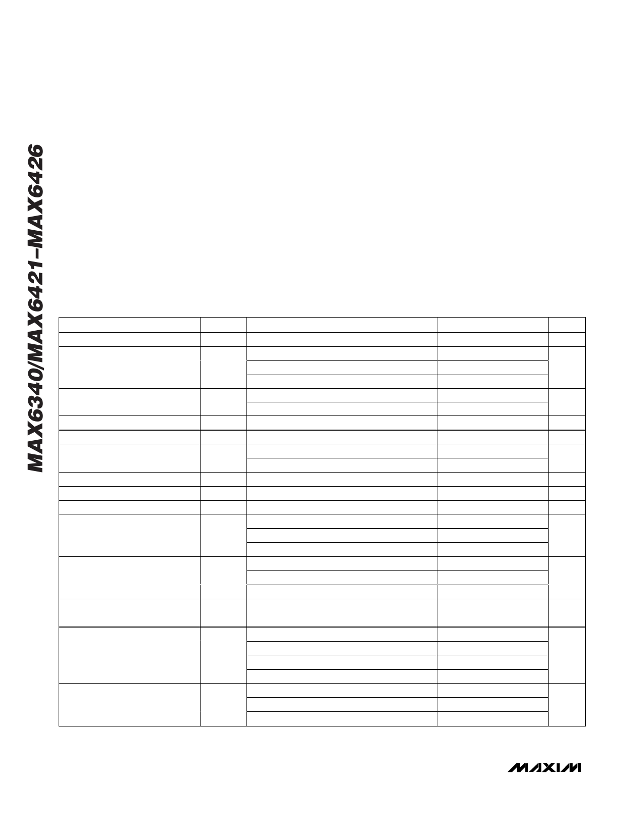
ELECTRICAL CHARACTERISTICS
(VCC = 1V to 5.5V, TA = TMIN to TMAX, unless otherwise specified. Typical values are at VCC = 5V and TA = +25В°C.) (Note 1)
PARAMETER
SYMBOL
CONDITIONS
MIN TYP MAX UNITS
Supply Voltage Range
Supply Current
VCC Reset Threshold Accuracy
Hysteresis
VCC to Reset Delay
Reset Timeout Period
VSRT Ramp Current
VSRT Ramp Threshold
RAMP Threshold Hysteresis
RESET Output Voltage Low
RESET Output Voltage High,
Push-Pull
RESET Output Leakage Current,
Open-Drain
VCC
ICC
VTH
VHYST
tRD
tRP
IRAMP
VTH-RAMP
VOL
VOH
VCC вүӨ 5.0V
VCC вүӨ 3.3V
VCC вүӨ 2.0V
TA = +25В°C
TA = -40В°C to +125В°C
VCC falling at 1mV/Вөs
CSRT = 1500pF
CSRT = 0
VSRT = 0 to 0.65V; VCC = 1.6V to 5V
VCC = 1.6V to 5V (VRAMP rising)
VRAMP falling threshold
VCC вүҘ 1.0V, ISINK = 50ВөA
VCC вүҘ 2.7V, ISINK = 1.2mA
VCC вүҘ 4.5V, ISINK = 3.2mA
VCC вүҘ 1.8V, ISOURCE = 200ВөA
VCC вүҘ 2.25V, ISOURCE = 500ВөA
VCC вүҘ 4.5V, ISOURCE = 800ВөA
ILKG VCC > VTH, reset not asserted
1.0
5.5
V
2.5
4.2
1.9
3.4
ВөA
1.6
2.5
VTH - 1.5%
VTH + 1.5%
V
VTH - 2.5% VTH + 2.5%
4 x VTH
mV
80
Вөs
3.00 4.375 5.75
ms
0.275
240
nA
0.65
V
33
mV
0.3
0.3
V
0.4
0.8 x VCC
0.8 x VCC
V
0.8 x VCC
1.0
ВөA
RESET Output Voltage High
RESET Output Voltage Low
VOH
VOL
VCC вүҘ 1.0V, ISOURCE = 1ВөA
VCC вүҘ 1.8V, ISOURCE = 150ВөA
VCC вүҘ 2.7V, ISOURCE = 500ВөA
VCC вүҘ 4.5V, ISOURCE = 800ВөA
VCC вүҘ 1.8V, ISINK = 500ВөA
VCC вүҘ 2.7V, ISINK = 1.2mA
VCC вүҘ 4.5V, ISINK = 3.2mA
0.8 x VCC
0.8 x VCC
0.8 x VCC
0.8 x VCC
V
0.3
0.3
V
0.4
Note 1: Devices production tested at +25В°C. Overtemperature limits are guaranteed by design.
2 _______________________________________________________________________________________
Share Link: