MAX6423US17-T жҹҘзңӢж•ёж“ҡиЎЁпјҲPDFпјү - Maxim Integrated
йӣ¶д»¶зј–еҸ·
дә§е“ҒжҸҸиҝ° (еҠҹиғҪ)
з”ҹдә§еҺӮ家
MAX6423US17-T
Maxim Integrated

MAX6423US17-T Datasheet PDF : 10 Pages
| |||
Low-Power, SC70/SOT ВөP Reset Circuits with
Capacitor-Adjustable Reset Timeout Delay
CSRT = (tRP - 275Вөs) / (2.73 вң• 106)
where tRP is in seconds and CSRT is in farads.
The reset delay time is set by a current/capacitor-con-
trolled ramp compared to an internal 0.65V reference.
An internal 240nA ramp current source charges the
external capacitor. The charge to the capacitor is
cleared when a reset condition is detected. Once the
reset condition is removed, the voltage on the capacitor
ramps according to the formula: dV/dt = I/C. The CSRT
capacitor must ramp to 0.65V to deassert the reset.
CSRT must be a low-leakage (<10nA) type capacitor;
ceramic is recommended.
Operating as a Voltage Detector
The MAX6340/MAX6421вҖ“MAX6426 can be operated in a
voltage detector mode by floating the SRT pin. The reset
delay times for VCC rising above or falling below the
threshold are not significantly different. The reset output is
deasserted smoothly without false pulses.
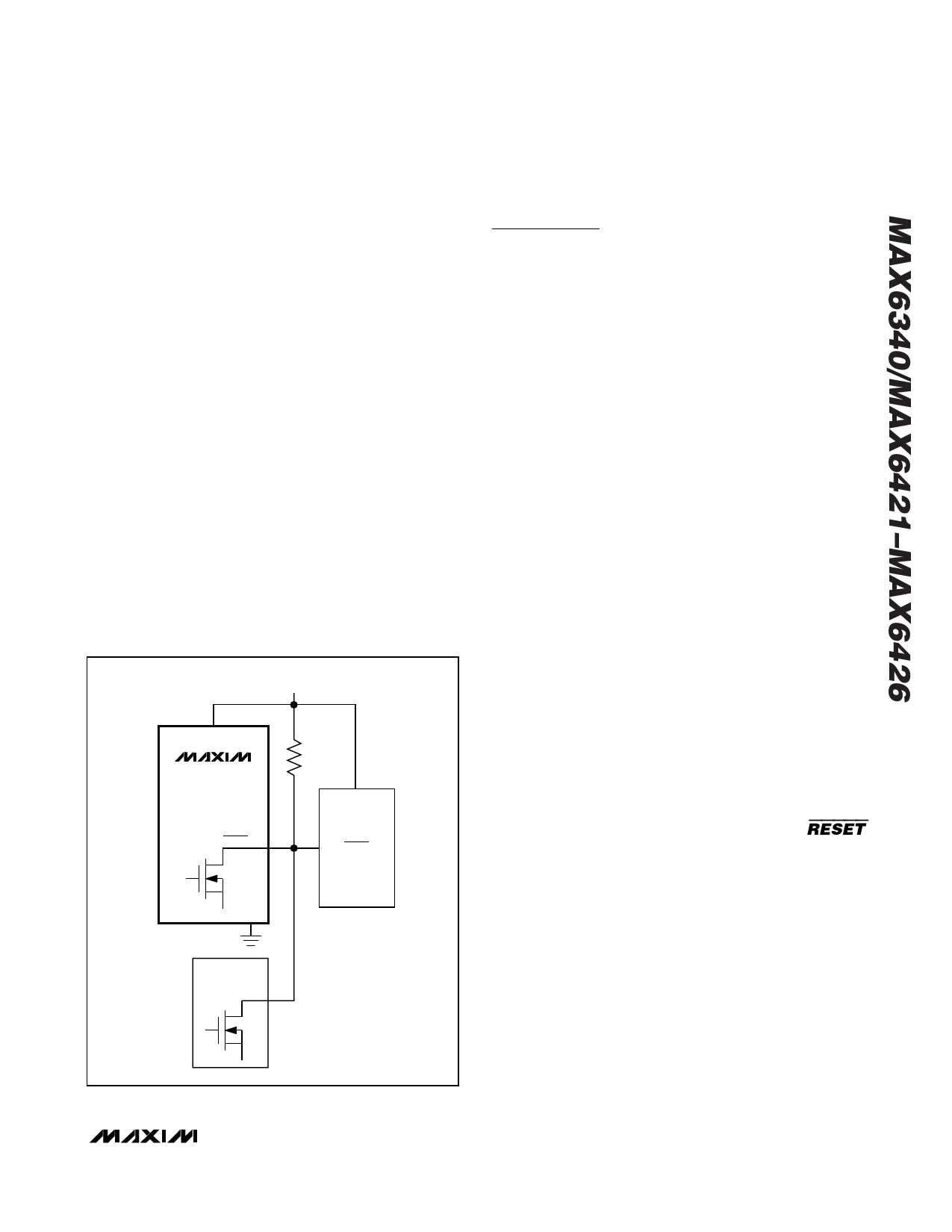
VCC
VDD
MAX6340
MAX6423
MAX6425
MAX6426
RESET
N
GND
10kв„Ұ
ВөP
RESET
OPEN-DRAIN
LOGIC
N
Figure 2. Wired-OR Reset Circuit
Applications Information
Interfacing to Other Voltages for Logic
Compatibility
The open-drain outputs of the MAX6340/MAX6423/
MAX6425/MAX6426 can be used to interface to ВөPs with
other logic levels. As shown in Figure 1, the open-drain
output can be connected to voltages from 0 to 5.5V. This
allows for easy logic compatibility to various ВөPs.
Wired-OR Reset
To allow auxiliary circuitry to hold the system in reset,
an external open-drain logic signal can be connected
to the open-drain RESET of the MAX6340/MAX6423/
MAX6425/MAX6426, as shown in Figure 2. This config-
uration can reset the ВөP, but does not provide the reset
timeout when the external logic signal is released.
Negative-Going VCC Transients
In addition to issuing a reset to the ВөP during power-up,
power-down, and brownout conditions, these supervisors
are relatively immune to short-duration negative-going
transients (glitches). The graph Maximum Transient
Duration vs. Reset Threshold Overdrive in the Typical
Operating Characteristics shows this relationship.
The area below the curve of the graph is the region in
which these devices typically do not generate a reset
pulse. This graph was generated using a negative-
going pulse applied to VCC, starting above the actual
reset threshold (VTH) and ending below it by the magni-
tude indicated (reset-threshold overdrive). As the mag-
nitude of the transient decreases (farther below the
reset threshold), the maximum allowable pulse width
decreases. Typically, a VCC transient that goes 100mV
below the reset threshold and lasts 50Вөs or less does
not cause a reset pulse to be issued.
Ensuring a Valid RESET or RESET
Down to VCC = 0
When VCC falls below 1V, RESET/RESET current-sink-
ing (sourcing) capabilities decline drastically. In the
case of the MAX6421/MAX6424, high-impedance
CMOS-logic inputs connected to RESET can drift to
undetermined voltages. This presents no problems in
most applications, since most ВөPs and other circuitry
do not operate with VCC below 1V.
In those applications where RESET must be valid down
to zero, adding a pulldown resistor between RESET
and ground sinks any stray leakage currents, holding
RESET low (Figure 3). The value of the pulldown resis-
tor is not critical; 100kв„Ұ is large enough not to load
RESET and small enough to pull RESET to ground. For
applications using the MAX6422, a 100kв„Ұ pullup resis-
_______________________________________________________________________________________ 5
Share Link: