MAX817M 查看數據表(PDF) - Maxim Integrated
零件编号
产品描述 (功能)
生产厂家
MAX817M Datasheet PDF : 16 Pages
| |||
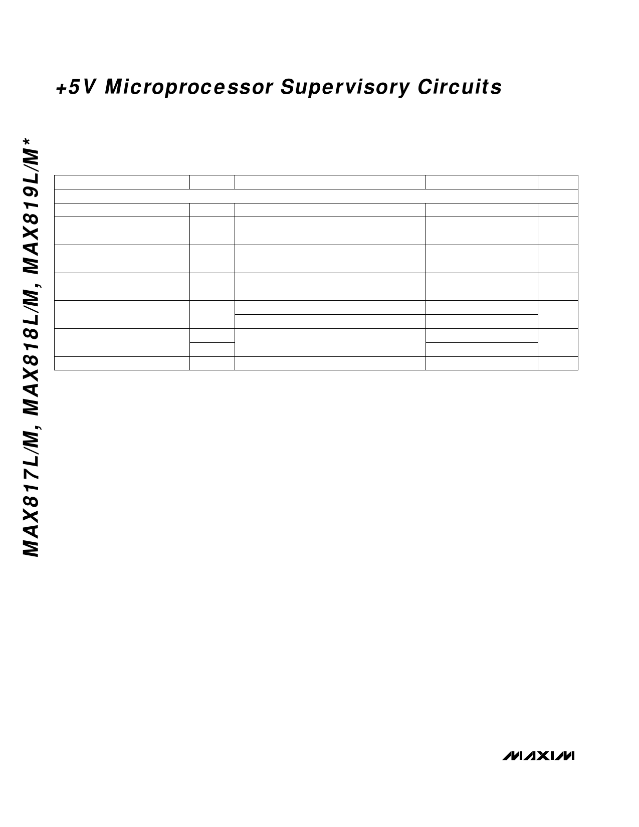
+5V Microprocessor Supervisory Circuits
ELECTRICAL CHARACTERISTICS (continued)
(VCC = +4.75V to +5.5V for MAX81_L, VCC = +4.5V to +5.5V for MAX81_M, VBATT = 2.8V, TA = TMIN to TMAX, unless otherwise
noted. Typical values are at TA = +25°C.)
PARAMETER
SYMBOL
CHIP-ENABLE GATING (MAX818 only)
CE IN Leakage Current
CONDITIONS
Disable mode
MIN TYP MAX UNITS
±0.005 ±1
µA
CE IN to CE OUT Resistance
(Note 6)
Enable mode
40
150
Ω
CE OUT Short-Circuit Current
(Reset Active)
Disable mode, CE OUT = 0V
0.1
0.75
2.0
mA
CE IN to CE OUT Propagation
Delay (Note 7)
50Ω source impedance driver, CLOAD = 50pF
3
8
ns
CE OUT Output
CE OUT Input Threshold
RESET to CE OUT Delay
VOH
VIH
VIL
IOUT = -100µA, VCC = 0V
IOUT = -1µA, VCC = 0V, VBATT = 2.8V
VCC = 5V
Power-down
VCC - 1V
V
2.7
0.8
V
3.5
15
µs
Note 2: Either VCC or VBATT can go to 0V if the other is greater than 2.0V.
Note 3: “-” = battery-charging current, “+” = battery-discharging current.
Note 4: WDI is internally serviced within the watchdog timeout period if WDI is left unconnected.
Note 5: WDI input is designed to be driven by a three-stated output device. To float WDI, the “high-impedance mode” of the output
device must have a maximum leakage current of 10µA and a maximum output capacitance of 200pF. The output device
must also be able to source and sink at least 200µA when active.
Note 6: The chip-enable resistance is tested with VCC = +4.75V for the MAX818L and VCC = +4.5V for the MAX818M.
V C E IN = V C E OUT = VCC/2.
Note 7: The chip-enable propagation delay is measured from the 50% point at CE IN to the 50% point at CE OUT.
4 _______________________________________________________________________________________
Share Link: 