MAX9779 查看數據表(PDF) - Maxim Integrated
零件编号
产品描述 (功能)
生产厂家
MAX9779 Datasheet PDF : 19 Pages
| |||
2.6W Stereo Audio Power Amplifier and
DirectDrive Headphone Amplifier
Table 1. MAX9779 Maximum Gain Settings
GAIN2
0
0
1
1
GAIN1
0
1
0
1
SPEAKER-MODE GAIN (dB)
15
16.5
18
19.5
HEADPHONE-MODE GAIN (dB)
0
0
3
3
Headphone Amplifier
In conventional single-supply headphone amplifiers,
the output-coupling capacitor is a major contributor of
audible clicks and pops. Upon startup, the amplifier
charges the coupling capacitor to its bias voltage, typical-
ly half the supply. Likewise, during shutdown, the capaci-
tor is discharged to GND. A DC shift across the capacitor
results, which in turn appears as an audible transient at
the speaker. Since the MAX9779 does not require output-
coupling capacitors, no audible transient occurs.
Additionally, the MAX9779 features extensive click-and-
pop suppression that eliminates any audible transient
sources internal to the device. The Power-Up/Down
Waveform in the Typical Operating Characteristics
shows that there are minimal spectral components in the
audible range at the output upon startup and shutdown.
Applications Information
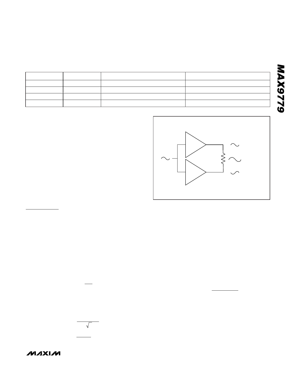
BTL Speaker Amplifiers
The MAX9779 features speaker amplifiers designed to
drive a load differentially, a configuration referred to as
bridge-tied load (BTL). The BTL configuration (Figure 6)
offers advantages over the single-ended configuration,
where one side of the load is connected to ground.
Driving the load differentially doubles the output volt-
age compared to a single-ended amplifier under similar
conditions. Thus, the device’s differential gain is twice
the closed-loop gain of the input amplifier. The effective
gain is given by:
AVD
=
2
×
RF
RIN
Substituting 2 x VOUT(P-P) into the following equation
yields four times the output power due to double the
output voltage:
VRMS = VOUT(P−P)
22
POUT
=
VRMS2
RL
+1
VOUT(P-P)
2 x VOUT(P-P)
-1
VOUT(P-P)
Figure 6. Bridge-Tied Load Configuration
Since the differential outputs are biased at midsupply,
there is no net DC voltage across the load. This elimi-
nates the need for DC-blocking capacitors required for
single-ended amplifiers. These capacitors can be large
and expensive, can consume board space, and can
degrade low-frequency performance.
Power Dissipation and Heatsinking
Under normal operating conditions, the MAX9779 can dis-
sipate a significant amount of power. The maximum power
dissipation for the TQFN package is given in the Absolute
Maximum Ratings under Continuous Power Dissipation,
or can be calculated by the following equation:
PDISSPKG(MAX)
=
TJ(MAX) −
θ JA
TA
where TJ(MAX) is +150°C, TA is the ambient tempera-
ture, and θJA is the reciprocal of the derating factor in
°C/W as specified in the Absolute Maximum Ratings
section. For example, θJA of the thin QFN package is
+42°C/W. For optimum power dissipation, the exposed
paddle of the package should be connected to the
ground plane (see the Layout and Grounding section).
______________________________________________________________________________________ 13
Share Link: 