MAX9779 查看數據表(PDF) - Maxim Integrated
零件编号
产品描述 (功能)
生产厂家
MAX9779 Datasheet PDF : 19 Pages
| |||
2.6W Stereo Audio Power Amplifier and
DirectDrive Headphone Amplifier
ABSOLUTE MAXIMUM RATINGS
Supply Voltage (VDD, PVDD, HPVDD, CPVDD to GND)..........+6V
GND to PGND.....................................................................±0.3V
CPVSS, C1N, VSS to GND .........................-6.0V to (GND + 0.3V)
HPOUT_ to GND ....................................................................±3V
Any Other Pin .............................................-0.3V to (VDD + 0.3V)
Duration of OUT_ _ Short Circuit to GND or PVDD .....Continuous
Duration of OUT_+ Short Circuit to OUT_- .................Continuous
Duration of HPOUT_ Short Circuit to GND,
VSS or HPVDD.........................................................Continuous
Continuous Current (PVDD, OUT_ _, PGND) ........................1.7A
Continuous Current (CPVDD, C1N, C1P, CPVSS, VSS, HPVDD,
HPOUT_) .......................................................................850mA
Continuous Input Current (all other pins) .........................±20mA
Continuous Power Dissipation (TA = +70°C)
28-Pin Thin QFN (derate 20.8mW/°C above +70°C) ..1667mW
Junction Temperature ......................................................+150°C
Operating Temperature Range ...........................-40°C to +85°C
Storage Temperature Range .............................-65°C to +150°C
Lead Temperature (soldering, 10s) .................................+300°C
Stresses beyond those listed under “Absolute Maximum Ratings” may cause permanent damage to the device. These are stress ratings only, and functional
operation of the device at these or any other conditions beyond those indicated in the operational sections of the specifications is not implied. Exposure to
absolute maximum rating conditions for extended periods may affect device reliability.
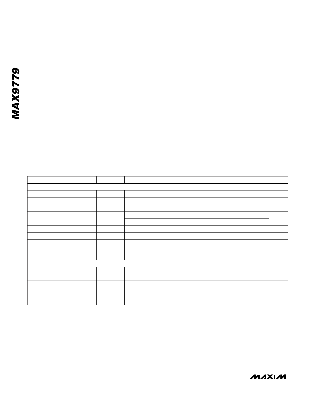
ELECTRICAL CHARACTERISTICS
(VDD = PVDD = CPVDD = HPVDD = 5V, GND = PGND = CPGND = 0V, SHDN = VDD, CBIAS = 1µF, C1 = C2 = 1µF, speaker load
terminated between OUT_+ and OUT_-, headphone load terminated between HPOUT_ and GND, GAIN1 = GAIN2 = 0V, TA = TMIN to
TMAX, unless otherwise noted. Typical values are at TA = +25°C.) (Note 1)
PARAMETER
GENERAL
Supply Voltage Range
Headphone Supply Voltage
SYMBOL
VDD, PVDD
CPVDD,
HPVDD
Quiescent Supply Current
IDD
Shutdown Supply Current
ISHDN
Bias Voltage
VBIAS
Switching Time
tSW
Input Resistance
RIN
Turn-On Time
tSON
SPEAKER AMPLIFIER (HPS = GND)
Output Offset Voltage
VOS
Power-Supply Rejection Ratio
(Note 3)
PSRR
CONDITIONS
Inferred from PSRR test
Inferred from PSRR test
HPS = GND, speaker mode, RL = ∞
HPS = VDD, headphone mode, RL = ∞
SHDN = GND
Gain or input switching
Amplifier inputs (Note 2)
Measured between OUT_+ and OUT_-,
TA = +25°C
PVDD or VDD = 4.5V to 5.5V (TA = +25°C)
f = 1kHz, VRIPPLE = 200mVP-P
f = 10kHz, VRIPPLE = 200mVP-P
MIN TYP MAX UNITS
4.5
5.5
V
3.0
5.5
V
14
29
mA
7
13
0.2
5
µA
1.7
1.8
1.9
V
10
µs
10
20
30
kΩ
25
ms
±1
±15
mV
75
90
80
dB
55
2 _______________________________________________________________________________________
Share Link: 