MB91314A 查看數據表(PDF) - Fujitsu
零件编号
产品描述 (功能)
生产厂家
MB91314A Datasheet PDF : 73 Pages
| |||
MB91314A Series
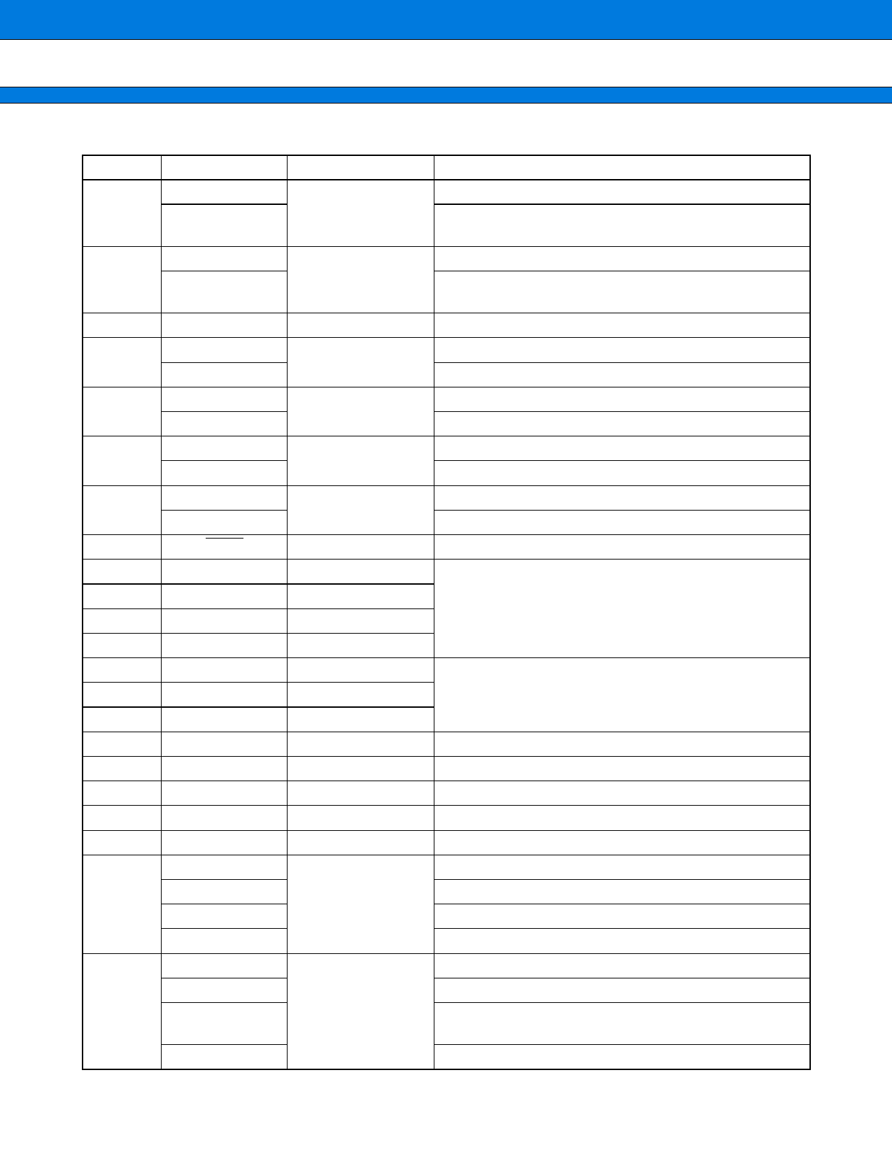
Pin no.
73
74
75
76
77
78
79
80
81
82
83
84
85
86
87
88
89
90
91
92
93
94
Pin name
PC1
SOT9/SDA9
PC2
SCK9/SCL9
PC3
PC4
PPGA
PC5
PPGB
PC6
TRG0
PC7
TRG1
TRST
ICD0
ICD1
ICD2
ICD3
ICS0
ICS1
ICS2
ICLK
IBREAK
VDDE
VSS
VDDI
P00
D00
SIN3
INT8
P01
D01
SOT3/SDA3
INT9
10
I/O circuit type*
B
B
B
B
B
B
B
G
K
K
K
K
H
H
H
H
I
⎯
⎯
⎯
C
C
Description
General-purpose I/O port
Multi function serial 9 serial data output pin
I2C data I/O pin
General-purpose I/O port
Multi function serial 9 serial communication clock I/O pin
I2C clock I/O pin
General-purpose I/O port
General-purpose I/O port
Output pin for PPG
General-purpose I/O port
Output pin for PPG
General-purpose I/O port
PPG trigger input
General-purpose I/O port
PPG trigger input
Reset pin for development tool
Data pin for development tool
Status pin for development tool
Clock pin for development tool
Break pin for development tool
3.3 V power supply
GND pin
1.8 V power supply
General-purpose I/O port
External address/ data bus I/O pin
Multi function serial 3 serial data input pin
External interrupt request input pin
General-purpose I/O port
External address/ data bus I/O pin
Multi function serial 3 serial data output pin
I2C data I/O pin
External interrupt request input pin
(Continued)
Share Link: 