MB95FV100D-103PBT 查看數據表(PDF) - Fujitsu
零件编号
产品描述 (功能)
生产厂家
MB95FV100D-103PBT Datasheet PDF : 74 Pages
| |||
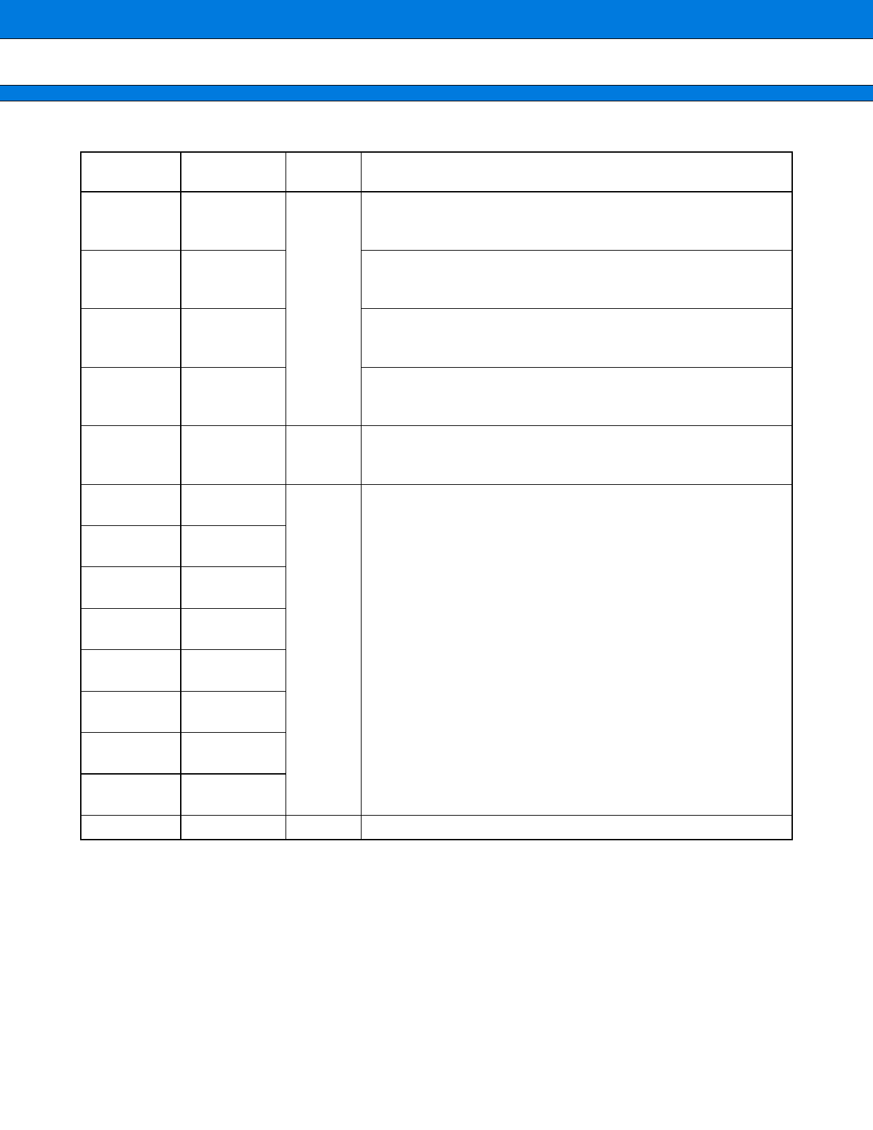
MB95160M Series
(Continued)
Pin no.
Pin name
I/O circuit
type*
Function
51
P63/SEG19/
TO11
General-purpose I/O port.
The pin is shared with LCDC SEG output (SEG19) and 8/16-bit
compound timer ch.1 output (TO11) .
52
P64/SEG20/
EC1
General-purpose I/O port.
The pin is shared with LCDC SEG output (SEG20) and 8/16-bit
compound timer ch.1 clock input (EC1) .
M
53
P65/SEG21/
SCK
General-purpose I/O port.
The pin is shared with LCDC SEG output (SEG21) and LIN-UART
clock I/O (SCK) .
54
P66/SEG22/
SOT
General-purpose I/O port.
The pin is shared with LCDC SEG output (SEG22) and LIN-UART
data output (SOT) .
55
P67/SEG23/
SIN
General-purpose I/O port.
N
The pin is shared with LCDC SEG output (SEG23) and LIN-UART
data input (SIN) .
56
P07/INT07/
AN07/SEG24
57
P06/INT06/
AN06/SEG25
58
P05/INT05/
AN05/SEG26
59
60
P04/INT04/
AN04/SEG27
P03/INT03/
AN03/SEG28
General-purpose I/O port.
F
The pins are shared with external interrupt input (INT00 to INT07) ,
A/D analog input (AN00 to AN07) and LCDC SEG output (SEG24 to
SEG31) .
61
P02/INT02/
AN02/SEG29
62
P01/INT01/
AN01/SEG30
63
P00/INT00/
AN00/SEG31
64
AVSS
⎯ Power supply pin (GND) of A/D converter
* : Refer to “■ I/O CIRCUIT TYPE” for details on the I/O circuit types.
10
Share Link: 