MB95FV100D-103PBT 查看數據表(PDF) - Fujitsu
零件编号
产品描述 (功能)
生产厂家
MB95FV100D-103PBT Datasheet PDF : 74 Pages
| |||
MB95160M Series
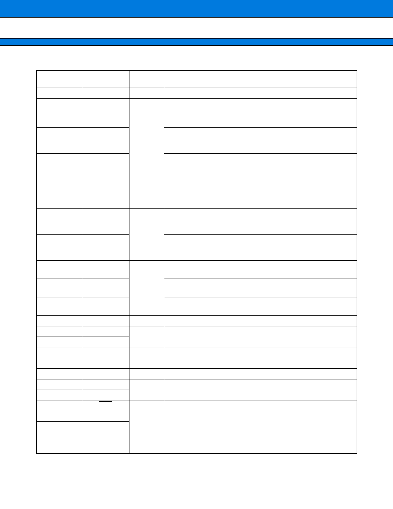
■ PIN DESCRIPTION
Pin no.
Pin name
1
AVCC
2
AVR
3
P14/PPG0
4
P13/TRG0/
ADTG
5
P12/UCK0
6
P11/UO0
7
P10/UI0
8
P24/EC0/
SDA0
9
P23/TO01/
SCL0
10
P22/TO00
11
P21/PPG01
12
P20/PPG00
13
MOD
14
X0
15
X1
16
VSS
17
VCC
18
C
19
X1A
20
X0A
21
RST
22
P90/V3
23
P91/V2
24
P92/V1
25
P93/V0
I/O circuit
type*
Function
⎯ A/D converter power supply pin
⎯ A/D converter reference input pin
General-purpose I/O port.
The pin is shared with 16-bit PPG ch.0 output.
General-purpose I/O port.
The pin is shared with 16-bit PPG ch.0 trigger input (TRG0) and
H
A/D converter trigger input (ADTG) .
General-purpose I/O port.
The pin is shared with UART/SIO ch.0 clock I/O.
General-purpose I/O port.
The pin is shared with UART/SIO ch.0 data output.
G
General-purpose I/O port.
The pin is shared with UART/SIO ch.0 data input.
General-purpose I/O port.
The pin is shared with 8/16-bit compound timer ch.0 clock input
(EC0) and I2C ch.0 data I/O (SDA0) .
I
General-purpose I/O port.
The pin is shared with 8/16-bit compound timer ch.0 output (TO01)
and I2C ch.0 clock I/O (SCL0) .
General-purpose I/O port.
The pin is shared with 8/16-bit compound timer ch.0 output.
H
General-purpose I/O port.
The pin is shared with 8/16-bit PPG ch.0 output.
General-purpose I/O port.
The pin is shared with 8/16-bit PPG ch.0 output.
B
Operating mode designation pin
A
Main clock oscillation pin
⎯ Power supply pin (GND)
⎯ Power supply pin
⎯ Capacitor connection pin
A
Sub clock oscillation pins (32 kHz)
B’ Reset pin
R
General-purpose I/O port.
The pins are shared with power supply pin for LCDC drive.
(Continued)
8
Share Link: 