MC1121 查看數據表(PDF) - ON Semiconductor
零件编号
产品描述 (功能)
生产厂家
MC1121 Datasheet PDF : 8 Pages
| |||
MC1121
+
C1
MC1121
“1”
Vin+
FC
1
CAP+
2
VDD 8
OSC
7
GND SHDN
3
6
4 CAP– Vout 5
SHDN*
+
C1n
C2
NOTES: *SHDN should be tied to it’s respective VDD if not used. +
MC1121
“n”
FC
1
CAP+
2
VDD 8
OSC
7
GND SHDN
3
6
4 CAP– Vout 5
SHDN*
Vout
C2
+
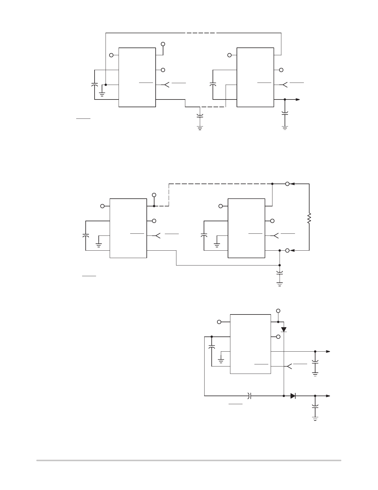
Figure 2. Cascading MC1121s to Increase Output Voltage
Paralleling Devices
To reduce output resistance, multiple MC1121s may be
paralleled (see Figure 3). Each device needs a pump
capacitor C1, but the reservoir capacitor C2 serves all
devices. The value of C2 should be increased by a factor of
n (the number of devices).
+
C1
MC1121
“1”
Vin+
FC
1
CAP+
2
VDD 8
OSC
7
OSC
GND SHDN
3
6
4 CAP– Vout 5
*SHDN
+
C1n
MC1121
“n”
FC
1
CAP+
2
VDD 8
OSC
7
GND SHDN
3
6
4 CAP– Vout 5
Rout = Rout (of MC1121)/n(number of devices)
NOTES: *SHDN should be tied to VDD if not used.
Figure 3. Paralleling MC1121s to Reduce Output Resistance
SHDN*
C2
+
Combined Positive Supply Multiplication and Negative
Voltage Conversion
Figure 4 shows this dual function circuit, in which
capacitors C1 and C2 perform pump and reservoir functions
to generate the negative voltage. Capacitors C2 and C4 are
the respective capacitors for the multiplied positive voltage.
This particular configuration leads to higher source
impedances of the generated supplies due to the finite
impedance of the common charge–pump driver.
Vin+
1
FC
VDD
MC1121
8
+2
C1
3
CAP+
GND
OSC
7
Vout 5
4 CAP–
SHDN
6
D1, D2 = 1N4148
D1
Vout = Vin–
C2
SHDN* +
Vout = (2Vin) –
C3
(VFD1) – (VFD2)
+
NOTES: *SHDN should be
tied to VDD if not used.
D2
+
C4
Figure 4. Combined Positive
Multiplier and Negative Converter
http://onsemi.com
4
Share Link: 