MC141585 查看數據表(PDF) - Motorola => Freescale
零件编号
产品描述 (功能)
生产厂家
MC141585 Datasheet PDF : 27 Pages
| |||
rows, to control the characters display format of that row
such as the character blinking, color intensity, character dou-
ble height and character double width function. In addition,
other control registers are located at row 15 such as window
control, frame function control. Four window control registers
for each of four windows together with four frame control
registers occupy the first 18 columns of row 15 space. These
control registers will be described on the “REGISTERS” sec-
tion. ROW 16, COL 0 - 4 contain special function registers
for pattern generation and page ROM selection.
User should handle the internal display RAM address
location with care especially for those rows with double
length alphanumeric symbols. For example, if row n is des-
tined to be double height on the memory map, the data dis-
played on screen row n and n+1 will be represented by the
data contained in the memory address of row n only. The
data of next row n+1 on the memory map will appear on the
screen of n+2 and n+3 row space and so on. Hence, it is not
necessary to throw in a row of blank data to compensate for
the double row action. User needs to take care of excessive
row of data in memory in order to avoid over running the lim-
ited number of row space on the screen.
There is difference for rows with double width alphanu-
meric symbols. Only the data contained in the even num-
bered columns of memory map will be shown, the odd
numbered columns will be ignored and not disclosed.
REGISTERS
(I) Display Register
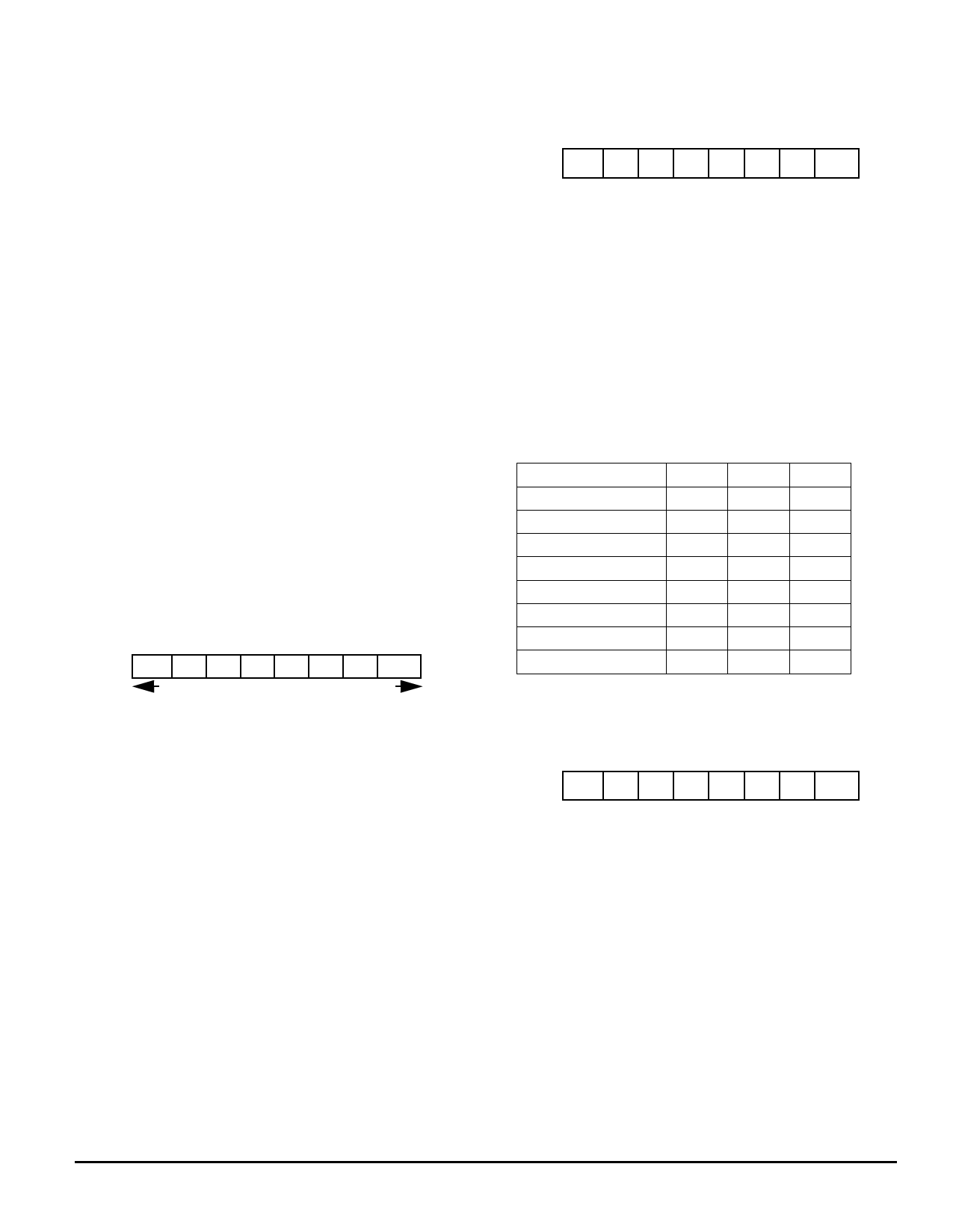
Display Register (Row 0~14, Coln 0~29)
7
6
54
32
1
0
CRADDR
Bit 7-0 CRADDR - This eight bits address one of the 256
characters or symbols resided in the 256 character ROM .
The 256 character ROM is compose of Bank A, Bank B and
Bank C. Bank A is fixed 128-ROM(address $00-$7F), Bank
B is first page 64-ROM(address $80-$BF) and Bank C is
second page 64-ROM(address $C0-$FF). Total addressable
ROM is 256 out of 512 physical ROM. Pages(Page 1 to
Page 6) in Bank B and Bank C can be selected by Page
Selection Register, ROW16 COL 4.
(II) Attribute Registers
Character Attribute Register (Row 0~14, Coln 0~29)
7
6
5
4
32
1
0
x BGR BGG BGB BLINK R G
B
Bit 6-4 These three bits define the color of the back-
ground for the correspondent characters. If all three bits are
clear, no background will be shown(transparent). Therefore,
total seven background colors can be selected.
Bit 7 Don’t Care.
Bit 3 BLINK - The blinking effect will be active on the
corresponding character if this bit is set to 1. The blinking
frequency is approximately one time per second (1Hz) with
fifty-fifty duty cycle at 80Hz vertical scan frequency.
Bit 2-0 These three bits are the color attribute to define
the color of the associated character/symbol.
Table 1. The Character/Window /Window shadow Color Selection
R
G
B
Black
0
0
0
Blue
0
0
1
Green
0
1
0
Cyan
0
1
1
Red
1
0
0
Magenta
1
0
1
Yellow
1
1
0
White
1
1
1
Row Attribute Register (Row 0~14, Coln 30)
7
6
5
4
32
1
0
R_INT CHS CWS
Bit 2 R_INT - Row intensity bit controls the color inten-
sity of the displayed character/symbol on the corresponding
row. Setting this bit to 0 means low intensity in this ROW and
R,G,B output voltage level will be equal to VDD(I). Set this bit
to 1 will switch the supply source of R,G,B back to VDD for
high intensity. Default setting is 0.
The low intensity function is not supported for the charac-
ters inside a high intensity windows and such characters will
still be high intensity even though R_INT is set 0. But inside
a low intensity window, the characters can be selected to
high or low intensity. Refer to W_INT bit description in the
window register for selecting the window intensity.
MOTOROLA
MC141585
9
Share Link: 