MC14489B 查看數據表(PDF) - Motorola => Freescale
零件编号
产品描述 (功能)
生产厂家
MC14489B Datasheet PDF : 22 Pages
| |||
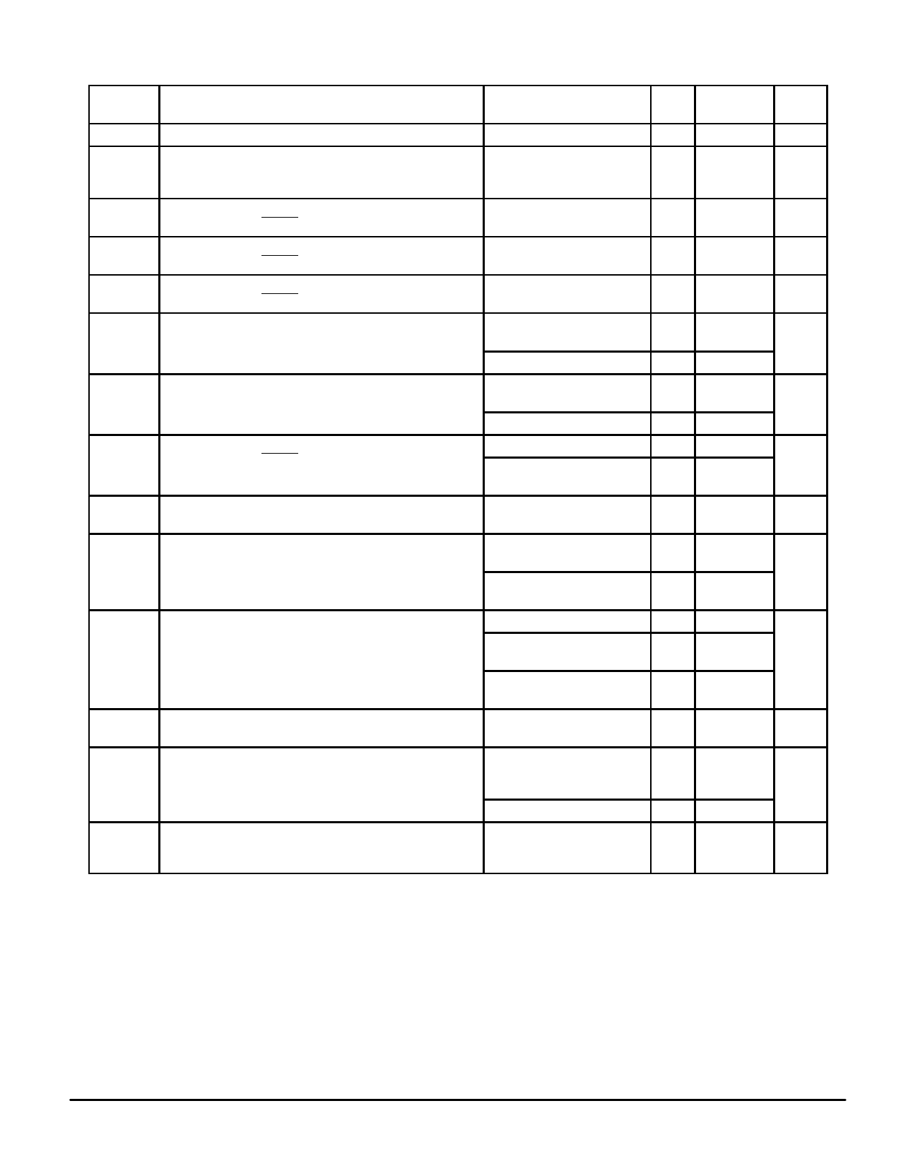
ELECTRICAL CHARACTERISTICS (Voltages Referenced to VSS, TJ = – 40° to 130°C* unless otherwise indicated)
Symbol
Parameter
Test Condition
VDD Guaranteed
V
Limit
Unit
VDD Power Supply Voltage Range of LED Drive Circuitry
VDD (stby) Minimum Standby Voltage
—
4.5 to 5.5
V
Bits Retained in Display and
—
3.0
V
Configuration Registers, Data
Port Fully Functional
VIL
Maximum Low–Level Input Voltage
(Data In, Clock, Enable)
3.0
0.9
V
5.5
1.65
VIH
Minimum High–Level Input Voltage
(Data In, Clock, Enable)
3.0
2.1
V
5.5
3.85
VHys
Minimum Hysteresis Voltage
(Data In, Clock, Enable)
3.0
0.2
V
5.5
0.4
VOL
Maximum Low–Level Output Voltage
(Data Out)
Iout = 20 µA
3.0
0.1
V
5.5
0.1
VOH
Minimum High–Level Output Voltage
(Data Out)
Iout = 1.3 mA
Iout = – 20 µA
4.5
0.4
3.0
2.9
V
5.5
5.4
Iin
Maximum Input Leakage Current
(Data In, Clock, Enable)
iOL
Minimum Sinking Current
(a, b, c, d, e, f, g, h)
Iout = – 800 µA
Vin = VDD or VSS
Vin = VDD or VSS,
TJ = 25°C only
Vout = 1.0 V
4.5
4.1
5.5
± 2.0
µA
5.5
± 0.1
4.5
0.2
mA
iOH
Peak Sourcing Current — See Figure 7 for currents up to Rx = 2.0 kΩ, Vout = 3.0 V,
35 mA (a, b, c, d, e, f, g, h)
Dimmer Bit = High
5.0 13 to 17.5
mA
Rx = 2.0 kΩ, Vout = 3.0 V,
5.0
6 to 9
Dimmer Bit = Low
IOZ
Maximum Output Leakage Current
(Bank 1, Bank 2, Bank 3, Bank 4, Bank 5)
Vout = VDD (FET Leakage)
5.5
50
µA
Vout = VDD (FET Leakage), 5.5
1
TJ = 25°C only
Vout = VSS (Protection Diode 5.5
1
Leakage)
Ron
Maximum ON Resistance
(Bank 1, Bank 2, Bank 3, Bank 4, Bank 5)
Iout = 0 to 200 mA
5.0
10
Ω
IDD, ISS Maximum Quiescent Supply Current
Device in Low–Power Mode, 5.5
100
µA
Vin = VSS or VDD, Rx in
Place, Outputs Open
Same as Above, TJ = 25°C
5.5
20
Iss
Maximum RMS Operating Supply Current
Device NOT in Low–Power
5.5
1.5
mA
(The VSS leg does not contain the Rx current component. Mode, Vin = VSS or VDD,
See Pin Descriptions.)
Outputs Open
* See Thermal Considerations section.
MOTOROLA
MC14489B
3
Share Link: 