MC33161 查看數據表(PDF) - ON Semiconductor
零件编号
产品描述 (功能)
生产厂家
MC33161 Datasheet PDF : 18 Pages
| |||
V4
Input VS2
V3
GND
Input −VS1
V1
V2
Output VCC
Voltage
Pins 5, 6 GND
MC34161, MC33161, NCV33161
VHys2
VHys1
LED ‘ON’
VCC
8
2.54V
1
Reference
−
R4 7
++
−VS1
+
2.8V
R3 2 + −
6
1.27V
−
R2
++
VS2
+
R1
3+ −
1.27V
0.6V
5
4
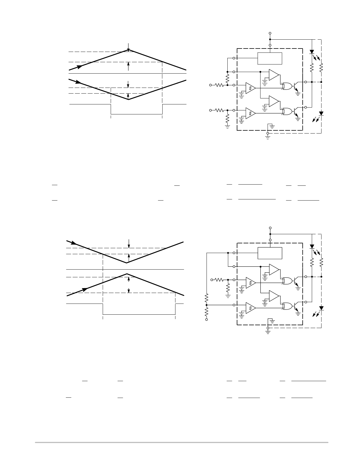
The above figure shows the MC34161 configured as a positive and negative overvoltage detector. As the input voltage increases from ground, the LED will turn
‘ON’ when either −VS1 exceeds V2, or VS2 exceeds V4. With the dashed line output connection, the circuit becomes a positive and negative undervoltage detector.
As the input voltage decreases from the peak towards ground, the LED will turn ‘ON’ when either VS2 falls below V3, or −VS1 falls below V1.
For known resistor values, the voltage trip points are:
V1
+
R3
R4
(Vth1
*
Vref)
)
Vth1
V2
+
R3
R4
(Vth1
*
VH1
*
Vref)
)
Vth1
*
VH1
ǒ Ǔ V3 + (Vth2 * VH2)
R2
R1
)
1
ǒ Ǔ V4 + Vth2
R2
R1
)
1
For a specific trip voltage, the required resistor ratio is:
R3
R4
+
(V1 * Vth1)
(Vth1 * Vref)
R3
R4
+
(V2 * Vth1 ) VH1)
(Vth1 * VH1 * Vref)
R2
R1
+
V4
Vth2
*
1
R2
R1
+
V3
Vth2 *
VH2
*
1
Figure 22. Positive and Negative Overvoltage Detector
Input VS1
V2
V1
GND
V3
Input −VS2
V4
Output VCC
Voltage
Pins 5, 6 GND
VHys1
VHys2
LED ‘ON’
VCC
8
2.54V
1
Reference
−
R4
VS1 R3
7
+
2+ −
1.27V
++
2.8V
−
6
R2
++
+
0.6V
R1
3+ −
1.27V
5
−VS2
4
The above figure shows the MC34161 configured as a positive and negative undervoltage detector. As the input voltage decreases toward ground, the LED will
turn ‘ON’ when either VS1 falls below V1, or −VS2 falls below V3. With the dashed line output connection, the circuit becomes a positive and negative overvoltage
detector. As the input voltage increases from the ground, the LED will turn ‘ON’ when either VS1 exceeds V2, or −VS1 exceeds V1.
For known resistor values, the voltage trip points are:
ǒ Ǔ V1 + (Vth1 * VH1)
R4
R3
)
1
ǒ Ǔ V2 + Vth1
R4
R3
)
1
V3
+
R1
R2
(Vth
*
Vref)
)
Vth2
V4
+
R1
R2
(Vth
*
VH2
*
Vref)
)
Vth2
*
VH2
For a specific trip voltage, the required resistor ratio is:
R4
R3
+
V2
Vth1
*
1
R4
R3
+
V1
Vth1 *
VH1
*
1
R1
R2
+
V4 ) VH2 * Vth2
Vth2 * VH2 * Vref
R1
R2
+
V3 * Vth2
Vth2 * Vref
Figure 23. Positive and Negative Undervoltage Detector
http://onsemi.com
11
Share Link: 