MC44817D 查看數據表(PDF) - Motorola => Freescale
零件编号
产品描述 (功能)
生产厂家
MC44817D Datasheet PDF : 8 Pages
| |||
MC44817/17B
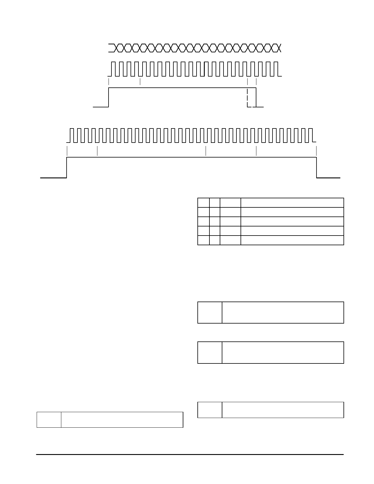
Bus Timing Diagram
Standard Bus Protocol 18 or 19 Bit
Data
1
45
18 19
Clock
Buffers
Frequency
Enable
Bus Protocol for Test and Features
1
45
19 20
26 27
33 34
B3 B2 B1 B0 N14 N13 N12 N11 N10 N9 N8 N7 N6 N5 N4 N3 N2 N1 N0 T6 T5 T4 T3 T2 T1 T0 X7 X6 X5 X4 X3 X2 X1 X0
Buffers
Frequency
Test & Features
Random
Definition of Permissible Bus Protocols
1. Bus Protocol for 18 Bit
B3 B2 B1 B0 N13 N12 N11 N10 N9 N8 N7 N6 N5 N4 N3
N2 N1 N0
Max Counting Ratio 16363
N14 is Reset Internally
2. Bus Protocol for 19 Bit
B3 B2 B1 B0 N14 N13 N12 N11 N10 N9 N8 N7 N6 N5 N4
N3 N2 N1 N0
Max Counting Ratio 32767
– B0 to B3: Control of Band Buffers
– N0 to N14: Control of Programmable Dividers
N14 = MSB; N0 = LSB
Minimum Counting Ratio Always 17
B3 = First Shifted Bit
N0 = Last Shifted Bit
3. Bus Protocol for Test and Further Features (34 Bit)
B3 B2 B1 B0 N14…N0 T6 T5 T4 T3 T2 T1 T0 X7
X6…X1 X0
– T0 to T3: Control the Phase Comparator
– T4: Switches Test Signals to the Buffer Outputs
– T5: Division Ratio of the Reference Divider
B Version T5 = “X”
– T6: Bypasses the Prescaler (Note 1)
– X0 to X7: Are Random
B3 = First Shifted Bit
X0 = Last Shifted Bit
Definition of the Bits for Test and Features
Bit T0: Defines the Charge Pump Current of the
Bit T0: Phase Comparator
T0 = 0
T0 = 1
Pump Current 50 µA Typical
Pump Current 15 µA Typical
6
Bits T1 and T2: Define the Digital Function of the Phase
Bits T1 and T2: Comparator
T2 T1 State Output Function of Phase Comparator
00
1
Normal Operation
01
2
High Impedance (Tri–State)
10
3
Upper Source “On”, Lower Source “Off”
11
4
Lower Source “On”, Upper Source “Off”
NOTE: 1. The phase comparator pulls high if the input frequency is too
high and it pulls low when the input frequency is too low.
(Inversion by Operational Amplifier) The phase comparator
generates a fixed duration offset pulse for each comparison
pulse (similar to the MC44802A). This guarantees operation in
the linear region. The offset pulse is a positive current pulse
(upper source).
Bit T3: Defines the Offset Pulse of the Phase
Bit T3: Comparator
T3 = 0
T3 = 1
Offset Pulse Short (200 ns)
Normal Mode
Offset Pulse Long (350 ns)
Bit T4: Switches the Internal Frequencies Fref and
Bit T4: FBY2 to the Buffer Outputs (B2, B3)
T4 = 0
T4 = 1
Normal Operation
Fref Switched to Buffer Output B2
FBY2 Switched to Buffer Output B3
NOTE:
Bits B2 and B3 have to be one in this case.
Fref is the reference frequency.
FBY2 is the output frequency of the programmable divider,
divided by two.
Bit T5: Defines the Division Ratio of the Reference
Bit T5: Divider
T5 = 0
T5 = 1
Division Ratio 512
Division Ratio 1024
NOTE: The division ratio of the reference divider can only be
programmed in the 34 bit bus protocol.
In the standard bus protocol the division ratio is 512.
(The power–up reset POR sets the division ratio to 512).
On “B–version”, T5 = “X”. Division ratio 1024 fixed.
MOTOROLA ANALOG IC DEVICE DATA
Share Link: 