MC44817D 查看數據表(PDF) - Motorola => Freescale
零件编号
产品描述 (功能)
生产厂家
MC44817D Datasheet PDF : 8 Pages
| |||
MC44817/17B
Bit T6: Switches the Prescaler
T6 = 0
T6 = 1
Normal Operation, 1.3 GHz
Low Frequency Operation
Preamp. 2 Switched Off, 165 MHz maximum
The prescaler is bypassed and the power supply of
the prescaler is switched off. Input: 10 MHz
minimum, 20 mVrms minimum
Figure 4. Equivalent Circuit of the Integrated
Band Buffers
25 V
Protection
Gnd IB
ISUB
VCC3 12 V
(Min VCC1, Max 14.4 V)
0.15 V Typical
0.3 V Max
“On”/“Off”
(1)
NOTE: IB + ISUB = 8.0 mA Typical, 13 mA Max
IB = Base Current
ISUB = Substrate Current of PNP
Out
B0…B3
30 mA (40 mA
at 0 to 80°C)
The Programmable Divider
The programmable divider is a presettable down counter.
When it has counted to zero it takes its required division ratio
out of the latches B. Latches B are loaded from latches A by
means of signal TDI which is synchronous to the
programmable divider output signal.
Since latches A receive the data asynchronously with the
programmable divider; this double latch scheme is needed to
assure correct data transfer to the counter.
The division ratio definition is given by:
N = 16384 x N14 + 8132 x N13 + … + 4 x N2 + 2 x N1 + N0
Maximum Ratio 32767
(16363 in case of 18 bit bus protocol)
Minimum Ratio 17
N0 … N14 are the different bits for frequency information.
At power–on the whole bus receiver is reset and the
programmable divider is set to a counting ratio of N = 256 or
higher.
The Prescaler
The prescaler has a preamplifier which guarantees high
input sensitivity.
The Phase Comparator
The phase comparator is phase and frequency sensitive
and has very low output leakage current in the high
impedance state.
The Operational Amplifier
The operational amplifier is designed for very low noise,
low input bias current and high power supply rejection. The
positive input is biased internally. The operational amplifier
needs 28.5 V supply (VCC2) as minimum voltage for a
guaranteed maximum tuning voltage of 28 V.
Figure 6 shows a possible filter arrangement. The
component values depend very much on the application
(tuner characteristic, reference frequency, etc.).
The Oscillator
The oscillator uses a 3.2 to 4.0 MHz crystal tied to ground in
series with a capacitor. The crystal operates in the series
resonance mode.
The voltage at Pin 3 has low amplitude and low harmonic
distortion.
Figure 5. Equivalent Circuit of the Lock Output
VCC1 5.0 V
200 µA Typical
2.0 k
Lock
100 k 25 V Protection
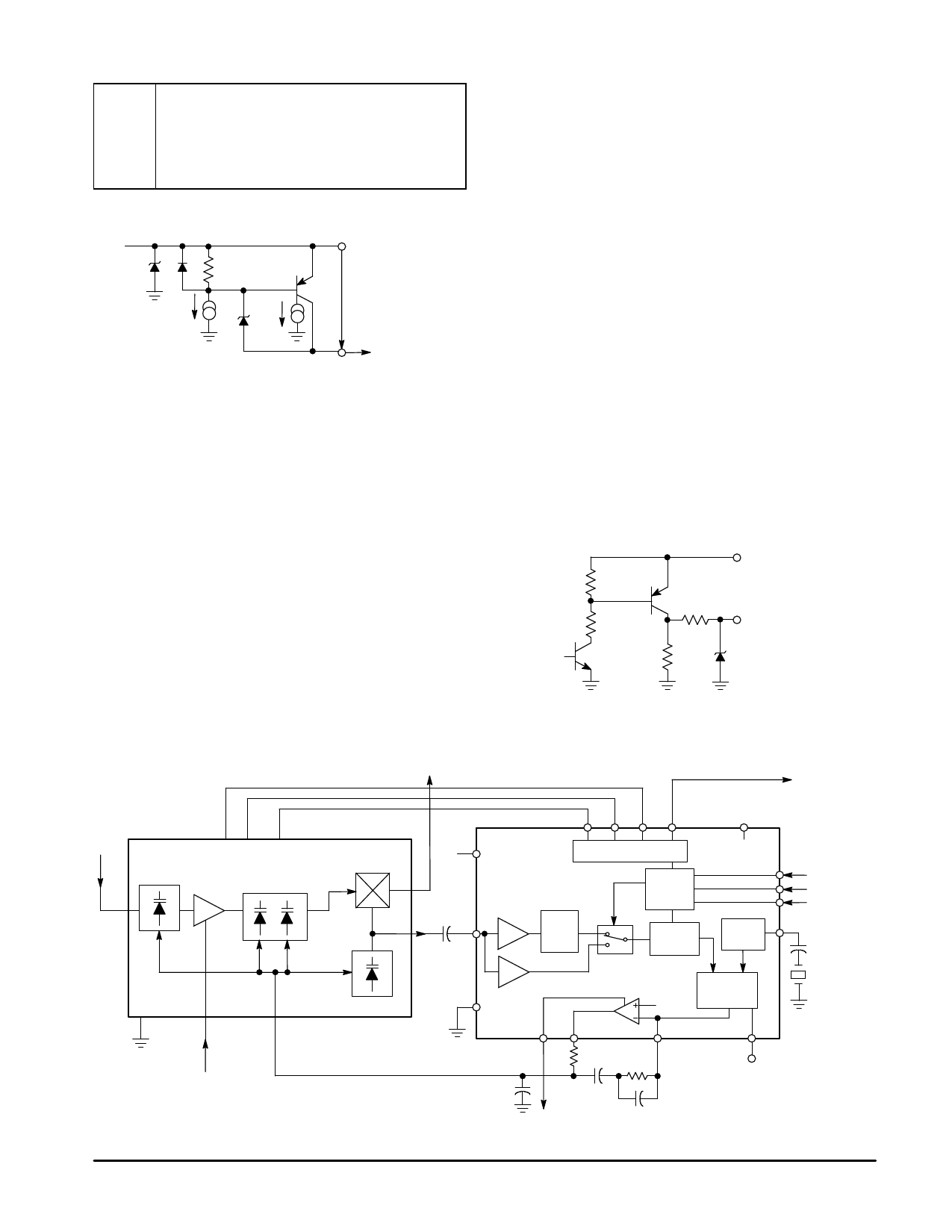
Figure 6. Typical Tuner Application
IF
UHF
External Switching
VHF B III
13 12 11 10
14 12 V
Antenna
Filter
B. P. Filter
Mixer
5.0 V 7
B3 B2 B1 B0
T6
MC44817/17B
Bus
Rec
1.0 nF 8
÷8
Pres
Fosc
Program
Divider
VCC3
2
1
16
Osc & 3
Ref Div
Oscillator
VTUN
AGC
NOTES: 1. On some layouts the 100 Ω resistor will not be required.
2. C2 = 330 pF minimum is required for stability.
Gnd
9
330 p
(Note 2)
2.7 V
65
4
(Note 1)
47 k
47 nF
33 V
22 nF
Phase
Comp
15
Lock
CL
DA
EN
12 pF
3.2/4.0 MHz
MOTOROLA ANALOG IC DEVICE DATA
7
Share Link: 