SA5222 查看數據表(PDF) - Philips Electronics
零件编号
产品描述 (功能)
生产厂家
SA5222 Datasheet PDF : 8 Pages
| |||
Philips Semiconductors
Low-power FDDI transimpedance amplifier
Product specification
SA5222
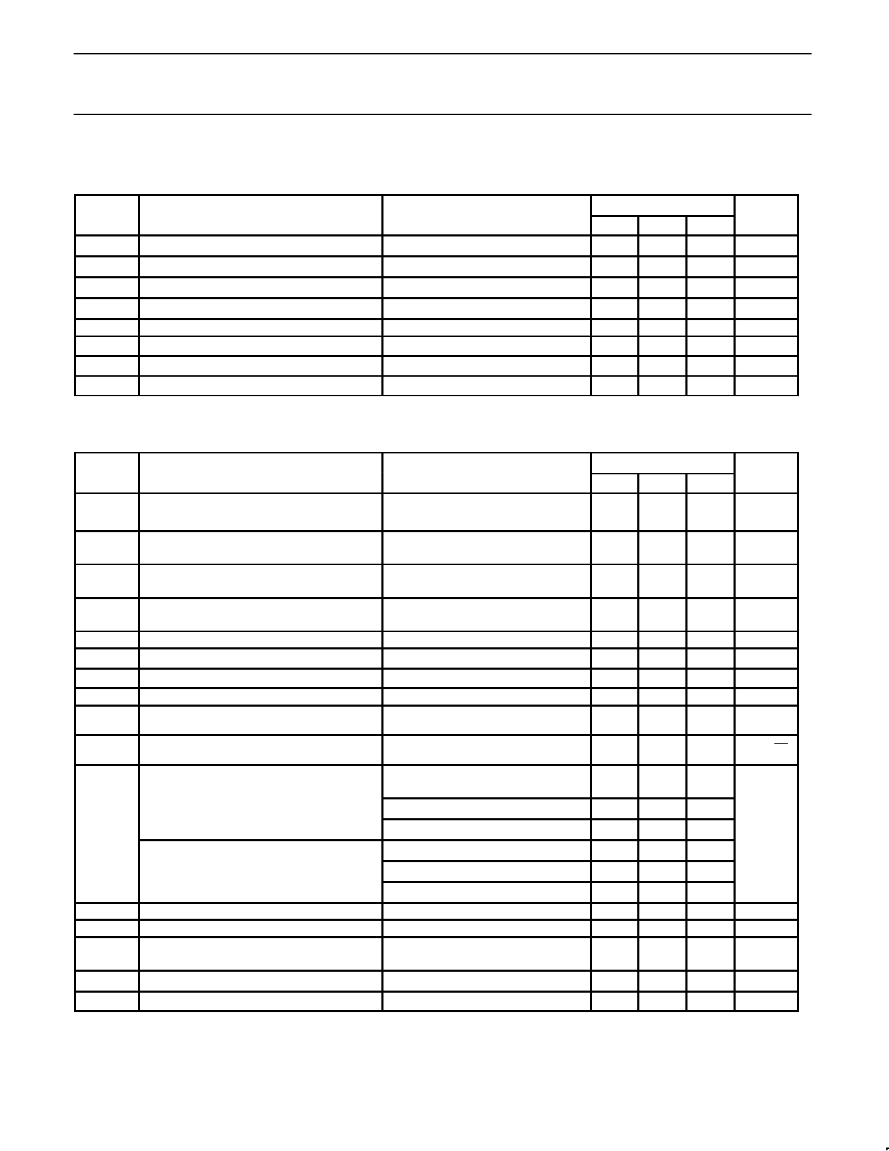
DC ELECTRICAL CHARACTERISTICS
Typical data and Min and Max limits apply at TA = 25°C, and VCC1 = VCC2 = +5V, unless otherwise specified.
SYMBOL
PARAMETER
TEST CONDITIONS
SA5222
Min Typ
VIN Input bias voltage
1.3 1.55
VO± Output bias voltage
2.9
3.2
VOS Output offset voltage
0
ICC Supply current
6
9
IOMAX
IIN
IINMAX
VOMAX
Output sink/source current
Input current (2% linearity)
Maximum input current overload threshold
Maximum differential output voltage swing
Test circuit 5, Procedure 2
Test circuit 5, Procedure 4
RL = ∞, Test Circuit 5, Procedure 3
1.5
2
±60 ±90
±80 ±115
3.6
Max
1.8
3.5
±100
12
UNIT
V
V
mV
mA
mA
µA
µA
VP-P
AC ELECTRICAL CHARACTERISTICS
Typical data and Min and Max limits apply at TA = 25°C and VCC1 = VCC2 =+5V, unless otherwise specified.
SYMBOL
PARAMETER
TEST CONDITIONS
SA5222
Min Typ Max
RT
Transresistance (differential output)
DC tested, RL = ∞, Test Circuit 5,
Procedure 1
13.3 16.6 19.9
UNIT
kΩ
RO
Output resistance
(differential output)
DC tested
30
60
90
Ω
RT
Transresistance
(single-ended output)
DC tested, RL = ∞
6.65 8.3 9.95
kΩ
RO
f3dB
RIN
CIN
∆R/∆V
∆R/∆T
IIN
IT
Output resistance
(single-ended output)
Bandwidth (-3dB)1
Input resistance
Input capacitance2
Transresistance power supply sensitivity
Transresistance ambient temperature sensi-
tivity
RMS noise current spectral density (referred
to input)
Integrated RMS noise current over the band-
width (referred to input)
CS = 0pF
CS = 1pF
DC tested
Test Circuit 1
VCC1 = VCC2 = 5 ±0.5V
∆TA = TA MAX - TA MIN
Test Circuit 2, f = 10MHz
Test circuit 2,
∆f = 50MHz
∆f = 100MHz
∆f = 150MHz
∆f = 50MHz
∆f = 100MHz
15
30
45
110 140
150
1
1.0
0.07
Ω
MHz
Ω
pF
%/V
%/oC
2.0
pAń ǸHz
15
25
36
nA
17
35
PSRR
PSRR
IINMAX
Power supply rejection ratio
Power supply rejection ratio3
Maximum input amplitude for output duty
cycle of 50 ±5%4
∆f = 150MHz
DC Tested, ∆VCC = ±0.5V
f = 1.0MHz, Test Circuit 3
Test circuit 4
55
–55
dB
–34
dB
±120
µA
tr, tf Rise and fall times
10 – 90%
2.2
ns
tD
Group delay
f = 10MHz
2.2
ns
NOTES:
1. Bandwidth is tested into 50Ω load. Bandwidth into 1kΩ load is approximately 165MHz.
2. Does not include Miller-multiplied capacitance of input device.
3. PSRR is output referenced and is circuit board layout dependent at higher frequencies. For best performance use a RF filter in VCC line.
4. Monitored in production via linearity and over load tests.
1995 Apr 26
2
Share Link: 