MC74HC139ADTR2G 查看數據表(PDF) - ON Semiconductor
零件编号
产品描述 (功能)
生产厂家
MC74HC139ADTR2G Datasheet PDF : 10 Pages
| |||
MC74HC139A
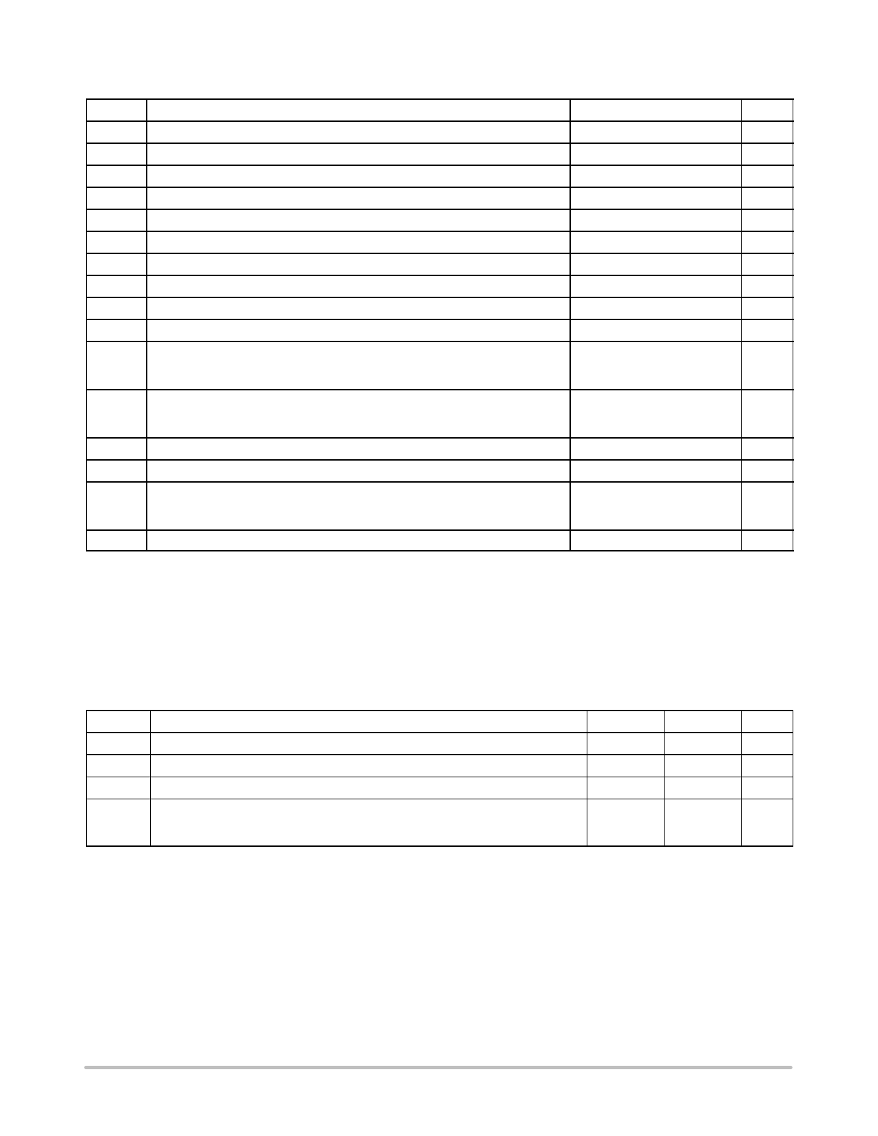
MAXIMUM RATINGS
Symbol
Parameter
Value
Unit
VCC
VIN
VOUT
IIN
IOUT
ICC
IGND
TSTG
TL
TJ
qJA
DC Supply Voltage
(Referenced to GND)
DC Input Voltage
(Referenced to GND)
DC Output Voltage
(Referenced to GND) (Note 1)
DC Input Current, per Pin
DC Output Current, per Pin
DC Supply Current, VCC Pin
DC Ground Current per Ground Pin
Storage Temperature Range
Lead Temperature, 1 mm from Case for 10 Seconds
Junction Temperature Under Bias
Thermal Resistance
PDIP
SOIC
TSSOP
*0.5 to )7.0
*1.5 to VCC )1.5
*0.5 to VCC )0.5
$20
$25
$50
$50
*65 to )150
260
)150
78
112
148
V
V
V
mA
mA
mA
mA
_C
_C
_C
_C/W
PD
Power Dissipation in Still Air at 85_C
PDIP
750
mW
SOIC
500
TSSOP
450
MSL Moisture Sensitivity
Level 1
FR
VESD
Flammability Rating
ESD Withstand Voltage
Oxygen Index: 30% − 35%
UL 94 V−0 @ 0.125 in
Human Body Model (Note 2)
u2000
V
Machine Model (Note 3)
u200
Charged Device Model (Note 4)
u1000
ILATCHUP Latchup Performance
Above VCC and Below GND at 85_C (Note 5)
$300
mA
Maximum ratings are those values beyond which device damage can occur. Maximum ratings applied to the device are individual stress limit
values (not normal operating conditions) and are not valid simultaneously. If these limits are exceeded, device functional operation is not implied,
damage may occur and reliability may be affected.
1. IO absolute maximum rating must be observed.
2. Tested to EIA/JESD22−A114−A.
3. Tested to EIA/JESD22−A115−A.
4. Tested to JESD22−C101−A.
5. Tested to EIA/JESD78.
6. For high frequency or heavy load considerations, see Chapter 2the ON Semiconductor High−Speed CMOS Data Book (DL129/D).
RECOMMENDED OPERATING CONDITIONS
Symbol
Parameter
Min
Max
Unit
ÎÎÎÎÎÎÎÎÎÎÎÎÎÎÎÎÎÎÎÎÎÎÎÎÎÎÎÎÎÎÎÎÎ VCC
DC Supply Voltage
(Referenced to GND)
2.0
6.0
V
ÎÎÎÎÎÎÎÎÎÎÎÎÎÎÎÎÎÎÎÎÎÎÎÎÎÎÎÎÎÎÎÎÎ VIN, VOUT DC Input Voltage, Output Voltage
(Referenced to GND)
0
VCC
V
ÎÎÎÎÎÎÎÎÎÎÎÎÎÎÎÎÎÎÎÎÎÎÎÎÎÎÎÎÎÎÎÎÎ TA
Operating Temperature, All Package Types
*55
)125
_C
ÎÎÎÎÎÎÎÎÎÎÎÎÎÎÎÎÎÎÎÎÎÎÎÎÎÎÎÎÎÎÎÎÎ tr, tf
Input Rise and Fall Time
ÎÎÎÎÎÎÎÎÎÎÎÎÎÎÎÎÎÎÎÎÎÎÎÎÎÎÎÎÎÎÎÎÎ (Figure 3)
VCC = 2.0 V
0
VCC = 4.5 V
0
VCC = 6.0 V
0
1000
ns
500
400
ÎÎÎÎÎÎÎÎÎÎÎÎÎÎÎÎÎÎÎÎÎÎÎÎÎÎÎÎÎÎÎÎÎ 7. Unused inputs may not be left open. All inputs must be tied to a high−logic voltage level or a low−logic input voltage level.
http://onsemi.com
3
Share Link: 