MC74LCX16374 查看數據表(PDF) - ON Semiconductor
零件编号
产品描述 (功能)
生产厂家
MC74LCX16374
ON Semiconductor

MC74LCX16374 Datasheet PDF : 8 Pages
| |||
MC74LCX16374
Low−Voltage CMOS 16−Bit
D−Type Flip−Flop
With 5 V−Tolerant Inputs and Outputs
(3−State, Non−Inverting)
The MC74LCX16374 is a high performance, non−inverting 16−bit
D−type flip−flop operating from a 2.3 V to 3.6 V supply. The device is
byte controlled. Each byte has separate Output Enable and Clock Pulse
inputs. These control pins can be tied together for full 16−bit operation.
High impedance TTL compatible inputs significantly reduce current
loading to input drivers while TTL compatible outputs offer improved
switching noise performance. A VI specification of 5.5 V allows
MC74LCX16374 inputs to be safely driven from 5.0 V devices.
The MC74LCX16374 consists of 16 edge−triggered flip−flops with
individual D−type inputs and 5.0 V−tolerant 3−state true outputs. The
buffered clocks (CPn) and buffered Output Enables (OEn) are common
to all flip−flops within the respective byte. The flip−flops will store the
state of individual D inputs that meet the setup and hold time
requirements on the LOW−to−HIGH Clock (CP) transition. With the
OE LOW, the contents of the flip−flops are available at the outputs.
When the OE is HIGH, the outputs go to the high impedance state. The
OE input level does not affect the operation of the flip−flops.
Features
• Designed for 2.3 to 3.6 V VCC Operation
• 6.2 ns Maximum tpd
• 5.0 V Tolerant − Interface Capability With 5.0 V TTL Logic
• Supports Live Insertion and Withdrawal
• IOFF Specification Guarantees High Impedance When VCC = 0 V
• LVTTL Compatible
• LVCMOS Compatible
• 24 mA Balanced Output Sink and Source Capability
• Near Zero Static Supply Current in All Three Logic States (20 mA)
Substantially Reduces System Power Requirements
• Latchup Performance Exceeds 500 mA
• ESD Performance: Human Body Model >2000 V;
Machine Model >200 V
• These are Pb−Free Devices*
http://onsemi.com
48
1
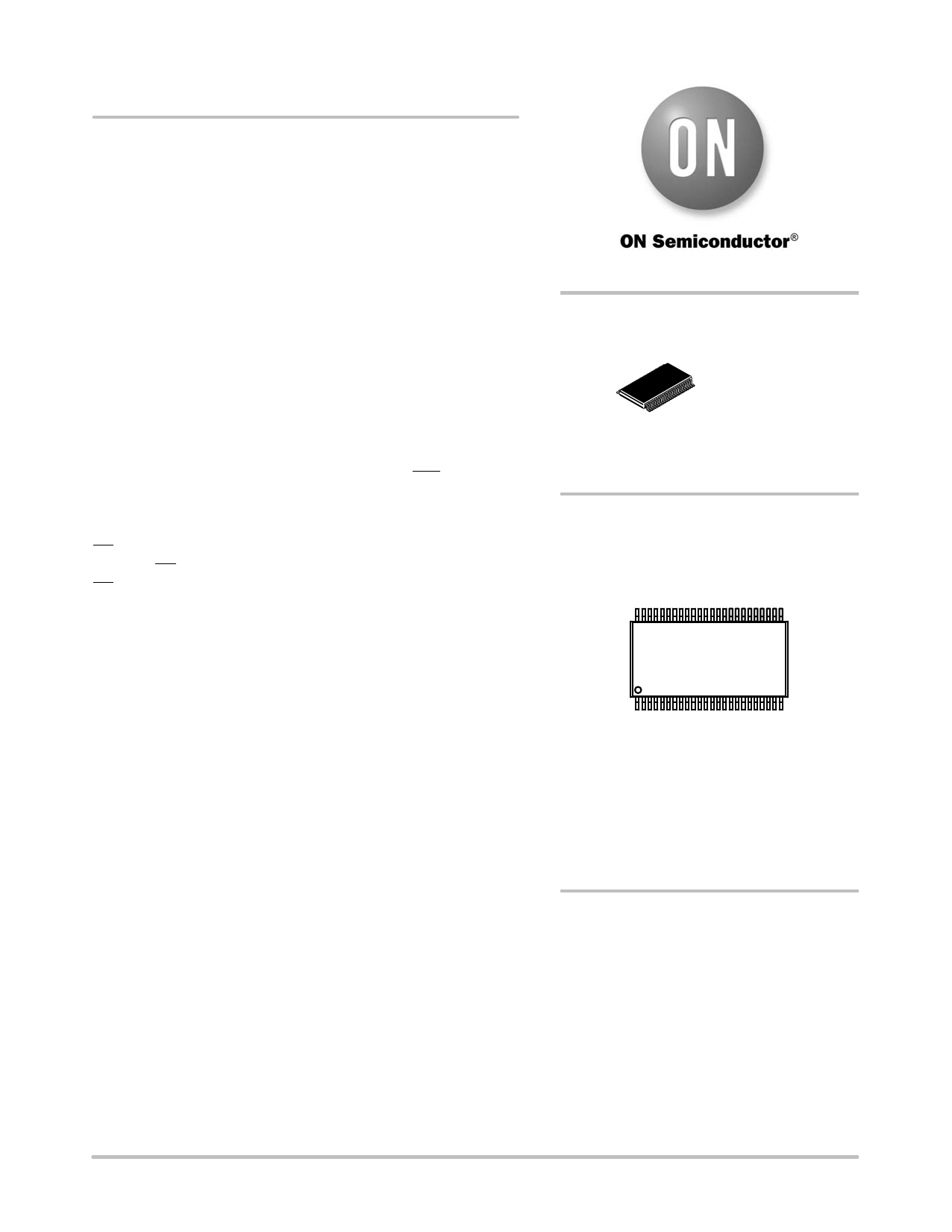
TSSOP−48
DT SUFFIX
CASE 1201
MARKING DIAGRAM
48
LCX16374G
AWLYYWW
1
A
= Assembly Location
WL = Wafer Lot
YY
= Year
WW = Work Week
G
= Pb−Free Package
ORDERING INFORMATION
See detailed ordering and shipping information in the package
dimensions section on page 3 of this data sheet.
*For additional information on our Pb−Free strategy and soldering details, please
download the ON Semiconductor Soldering and Mounting Techniques
Reference Manual, SOLDERRM/D.
© Semiconductor Components Industries, LLC, 2005
1
August, 2005 − Rev. 6
Publication Order Number:
MC74LCX16374/D
Share Link: