MCP23016 查看數據表(PDF) - Microchip Technology
零件编号
产品描述 (功能)
生产厂家
MCP23016 Datasheet PDF : 38 Pages
| |||
MCP23016
1.2 Power-on Reset (POR)
The on-chip POR circuit holds the chip in RESET until
VDD has reached a high enough level to deactivate the
POR circuit (i.e., release RESET). A maximum rise
time for VDD is specified in the electrical specifications.
When the device starts normal operation (exits the
RESET condition), device operating parameters
(voltage, frequency, temperature) must be met to
ensure proper operation.
1.3 Power-up Timer (PWRT)
The Power-up Timer provides a 72 ms nominal time-
out on power-up, keeping the device in RESET and
allowing VDD to rise to an acceptable level.
The power-up time delay will vary from chip-to-chip due
to VDD, temperature and process variation. See
Table 2-4 for details (TPWRT, parameter 3).
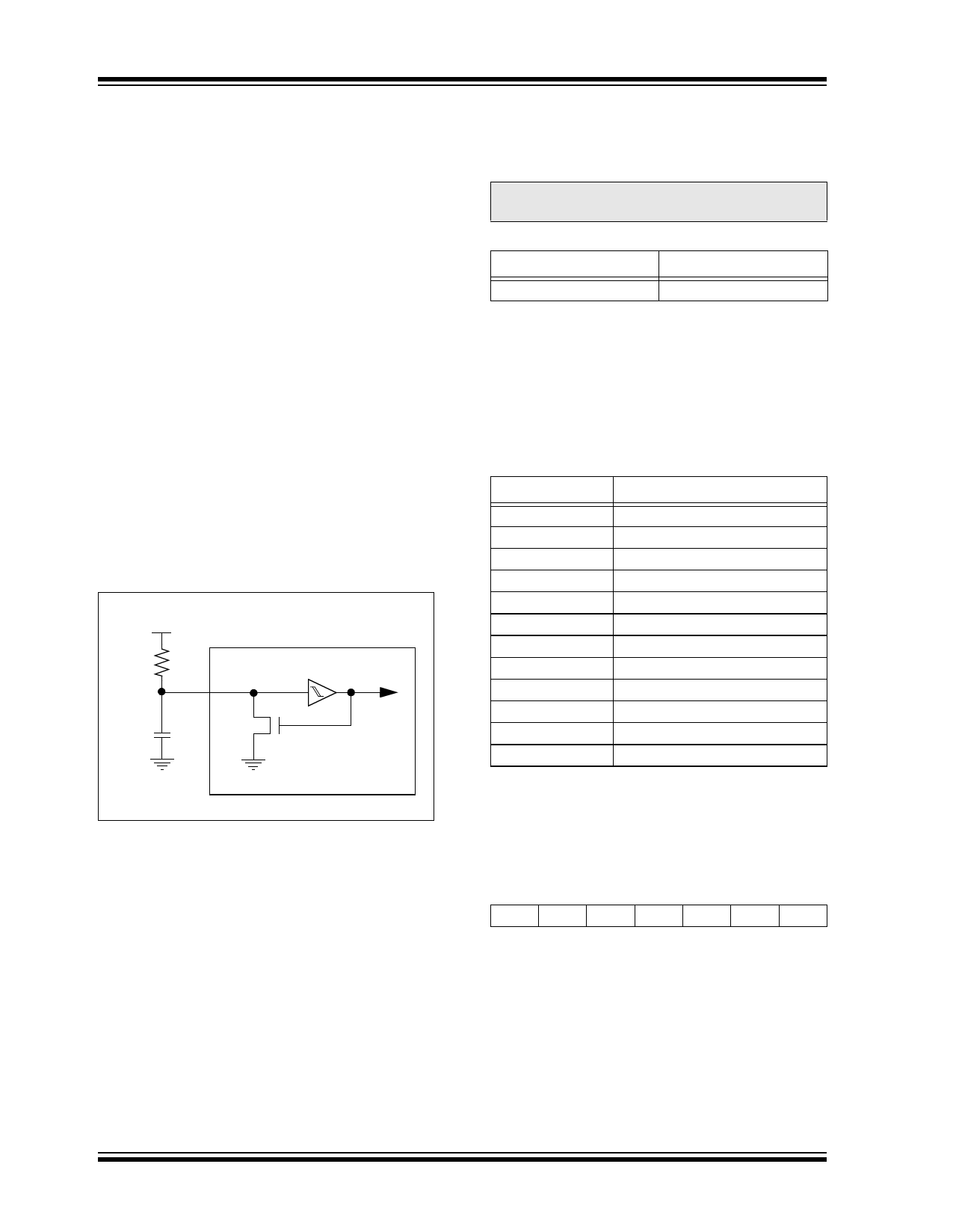
1.4 Clock Generator
The MCP23016 uses an external RC circuit to
determine the internal clock speed. The user must
connect R and C to the MCP23016, as shown in
Figure 1-1.
FIGURE 1-1:
CLOCK CONFIGURATION
VDD
REXT
CLK
Internal Clock
CEXT
VSS
MCP23016
A 1 MHz (typ.) internal clock is needed for the device to
function properly. The internal clock can be measured
on the TP pin. Recommended REXT and CEXT values
are shown in Table 1-2.
Note: Set IARES = 1 to measure the clock
output on TP.
TABLE 1-2: RECOMMENDED VALUES
REXT
CEXT
3.9 kΩ
33 pF
1.5 I2C Bus Interface/ Protocol
Handler
This block manages the functionality of the I2C bus
interface and protocol handling. The MCP23016
supports the following commands:
TABLE 1-3: COMMAND BYTE TO
REGISTER RELATIONSHIP
Command Byte
Result
0h
Access to GP0
1h
Access to GP1
2h
Access to OLAT0
3h
Access to OLAT1
4h
Access to IPOL0
5h
Access to IPOL1
6h
Access to IODIR0
7h
Access to IODIR1
8h
Access to INTCAP0 (Read-Only)
9h
Access to INTCAP1 (Read-Only)
Ah
Access to IOCON0
Bh
Access to IOCON1
1.6 Address Decoder
The last three LSb of the 7-bit address are user-defined
(see Table 1-4). Three hardware pins (<A2:A0>) define
these bits.
TABLE 1-4: DEVICE ADDRESS
0
1
0
0 A2 A1 A0
DS20090C-page 4
© 2007 Microchip Technology Inc.
Share Link: 