MCP607 查看數據表(PDF) - Microchip Technology
零件编号
产品描述 (功能)
生产厂家
MCP607 Datasheet PDF : 30 Pages
| |||
4.0 APPLICATIONS INFORMATION
The MCP606/7/8/9 family of op amps is manufactured
using Microchip’s state-of-the-art CMOS process
These op amps are unity-gain stable and suitable for a
wide range of general purpose applications.
4.1 Inputs
The MCP606/7/8/9 op amps are designed to prevent
phase reversal when the input pins exceed the supply
voltages. Figure 2-23 shows the input voltage
exceeding the supply voltage without any phase rever-
sal.
The inputs of the MCP606/7/8/9 op amps connect to a
differential PMOS input stage. The Common Mode
Input Voltage Range (VCMR) includes ground in single-
supply systems (VSS), but does not include VDD. This
means that the amplifier input behaves linearly as long
as the Common Mode Input Voltage (VCM) is kept within
the specified VCMR limits (VSS – 0.3V to VDD – 1.1V at
+25°C).
Input voltages that exceed the Absolute Maximum
Voltage Range (VSS – 0.3V to VDD + 0.3V) can cause
excessive current to flow into or out of the input pins.
Current beyond ±2 mA can cause reliability problems.
Applications that exceed this rating must be externally
limited with a resistor, as shown in Figure 4-1.
RIN
MCP60X
VIN
VOUT
RI
N
≥
-(--M-----a---x---i-m-----u---m------e--x---p---e---c--t--e---d----V----I--N---)----–----V----D----D--
2 mA
RIN
≥
V----S---S----–-----(--M-----i--n---i-m-----u---m-----e---x---p---e--c---t--e--d-----V----I--N----)
2 mA
FIGURE 4-1:
Resistor (RIN).
Input Current-Limiting
4.2 Rail-to-Rail Output
There are two specifications that describe the output-
swing capability of the MCP606/7/8/9 family of op amps.
The first specification (Maximum Output Voltage Swing)
defines the absolute maximum swing that can be
achieved under the specified load conditions. For
instance, the output voltage swings to within 15 mV of
the negative rail with a 25 kΩ load to VDD/2. Figure 2-23
shows how the output voltage is limited when the input
goes beyond the linear region of operation.
The second specification that describes the output-
swing capability of these amplifiers (Linear Output
Voltage Range) defines the maximum output swing that
can be achieved while the amplifier still operates in its
© 2005 Microchip Technology Inc.
MCP606/7/8/9
linear region. To verify linear operation in this range, the
large-signal DC Open-Loop Gain (AOL) is measured at
points inside the supply rails. The measurement must
meet the specified AOL conditions in the specification
table.
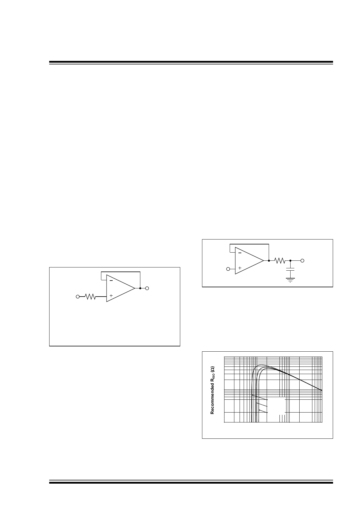
4.3 Capacitive Loads
Driving large capacitive loads can cause stability
problems for voltage-feedback op amps. As the load
capacitance increases, the feedback loop’s phase
margin decreases and the closed-loop bandwidth is
reduced. This produces gain-peaking in the frequency
response, with overshoot and ringing in the step
response. A unity-gain buffer (G = +1) is the most
sensitive to capacitive loads, though all gains show the
same general behavior.
When driving large capacitive loads with these op
amps (e.g., > 60 pF when G = +1), a small series
resistor at the output (RISO in Figure 4-2) improves the
feedback loop’s phase margin (stability) by making the
output load resistive at higher frequencies. The
bandwidth will be generally lower than the bandwidth
with no capacitive load.
MCP60X
VIN
RISO
CL
VOUT
FIGURE 4-2:
Output Resistor, RISO
stabilizes large capacitive loads.
Figure 4-3 gives recommended RISO values for
different capacitive loads and gains. The x-axis is the
normalized load capacitance (CL/GN), where GN is the
circuit’s noise gain. For non-inverting gains, GN and the
Signal Gain are equal. For inverting gains, GN is
1+|Signal Gain| (e.g., -1 V/V gives GN = +2 V/V).
10k10000
1k1000
GN = +1
GN = +2
GN t +4
100
100
10
10p
100
100p
1000
1n
10000
10n
Normalized Load Capacitance; CL/GN (F)
FIGURE 4-3:
Recommended RISO Values
for Capacitive Loads.
DS11177D-page 11
Share Link: 