MT90820AL 查看數據表(PDF) - Mitel Networks
零件编号
产品描述 (功能)
生产厂家
MT90820AL Datasheet PDF : 10 Pages
| |||
MT90820 CMOS
Advance Information
Serial Data Interface
The master clock (CLK) can be either at 4.096, 8.192
or 16.384 MHz allowing serial data link operation at
2.048, 4.096 and 8.192 Mb/s respectively. The
master clock frequency is always twice the data rate.
The input and output streams accept identical data
rate.
The input 8 kHz frame pulse can be in either ST-BUS
or GCI format. The LDX automatically detects the
presence of an input frame pulse and identifies the
type of serial interface. In ST-Bus format, every
second falling edge of the master clock marks a bit
boundary and the input data is clocked by the rising
edge, three quarters of the way into the bit cell. In
GCI format, every second rising edge of the master
clock marks the bit boundary while data sampling is
performed on the falling edge, at three quarters of
the bit cell boundary.
Switching Configuration
Switching configurations are determined basically by
the data rates selected at the serial inputs and
outputs. To specify the switching configuration
required, the Interface Mode Selection (IMS) register
has to be initialized on system power-up. The
switching configuration is selected by two DR bits in
the IMS register.
Serial Links with Data Rates at 2.048 Mb/s
When the 2.048Mb/s data rate is selected for input
and output streams, the device is configured with 16-
input/16-output data streams with 32 64Kbit/s
channels each. The modes allows 512 x 512 channel
Switch Matrix configuration. The interface clock is
4.096 MHz.
Serial Links with Data Rates at 4.096 Mb/s
When the 4.096 Mb/s data rate is selected for input
and output streams, the device is configured with 16-
input/16-output data streams with 64 64Kbit/s
channels each. The modes allows 1,024 x 1,024
channel Switch Matrix configuration. The interface
clock is 8.192MHz.
Serial Links with Data Rates at 8.192 Mb/s
When the 8.192Mb/s data rate is selected for input
and output streams, the device is configured with 16-
input/16-output data streams with 128 64Kbit/s
channels each. The modes allows 2,048 x 2,048
channel Switch Matrix configuration. The interface
clock is at 16.384 MHz.
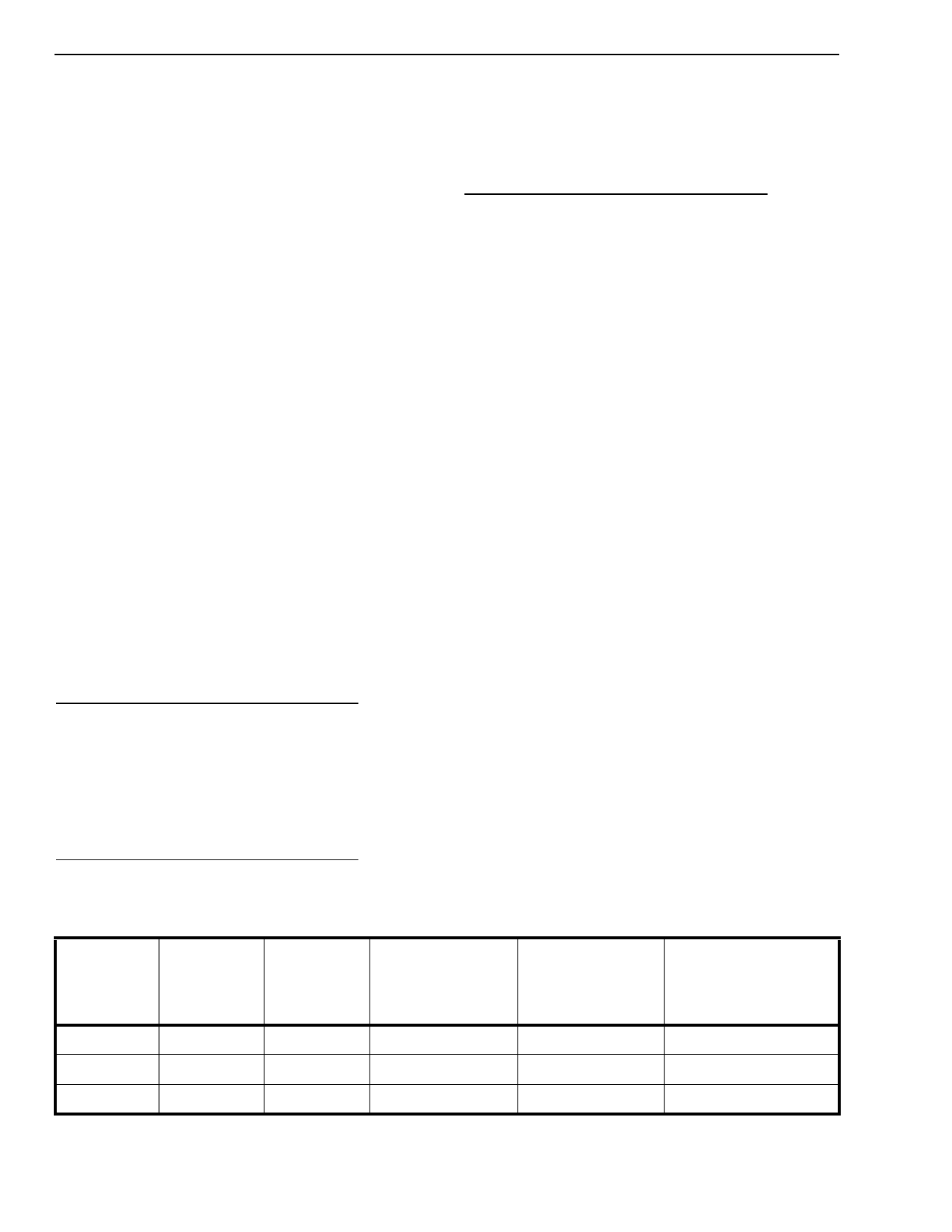
Table 1 summarizes the switching configurations.
Input Frame Offset Selection
The LDX provides a feature called Input Frame
Offset allowing users to compensate for the varying
delays on the incoming serial inputs while building
large switch matrices. Usually, different delays occur
on the digital backplanes causing the data and frame
pulse signal to be skewed at the input of the switch
device. This may result in the system frame pulse to
be active at the FRM input before the first bit of the
frame is received at the serial input.
The LDX allows users to compensate the input delay
offset by programming the Frame Input Offset (FOS)
registers. Each input stream can have its own delay
offset value. Possible adjustment is up to 4 master
clock periods forward with resolution of 1/2 clock
period.
Frame Alignment Evaluation
To manage the problem of different data input delays
(with respect to the frame pulse), the LDX provides
the FE input for the frame alignment evaluation. The
evaluation starts when the SFE bit in the IMS
register is changed from low to high. Two frames
later, the CFE bit of the frame alignment register
(FAR) changes from low to high to signal the CPU
Serial
Interface
Data Rate
2 Mb/s
4 Mb/s
8 Mb/s
Master
Clock
Required
(MHz)
4.096
8.192
16.384
Number of
Input x
Output
Streams
Matrix Channel
Capacity
Switch Matrix type
16 x 16
512 x 512
Non-Blocking
16 x 16
1,024 x 1,024
Non-Blocking
16 x 16
2,048 x 2,048
Non-Blocking
Table 1: Switching Configuration
Input/Output Stream
used
STi0-15/STo0-15
STi0-15/STo0-15
STi0-15/STo0-15
2-184
Share Link: 