MIC2551A(2004) 查看數據表(PDF) - Micrel
零件编号
产品描述 (功能)
生产厂家
MIC2551A Datasheet PDF : 11 Pages
| |||
MIC2551A
Power Supply Configuration
The MIC2551A can be set up for different power supply
configurations which modify the behavior of the device. Both
VBUS and VIF have special thresholds that detect when they
are either removed or grounded. Table 3 depicts the behavior
under the different power supply configuration scenarios that
are explained below.
Normal Mode
VBUS is connected to the 5.0V USB bus voltage and VIF is
connected to a supply voltage in the range of 1.6V to 3.6V. In
this case VTRM supplies a 3.3V voltage for powering the
speed select resistor via VPU depending on the state of CON
pin.
Disconnect Mode
VIF is connected to a supply in a range of 1.6V to 3.6V and
VBUS is open or grounded. If VBUS is opened while transmit-
ting, the data lines (D+, D–) have sharing capability and may
be driven with external devices up to approximately 3.6V if
and only if SUSPEND is enabled (SUS = 1). With VBUS
ground, D+, D– sharing mode is not permitted.
Disable Mode
VBUS is connected to the 5.0V USB bus voltage and VIF is
open. All logic controlled inputs become high impedances,
thus minimal current will be supplied by VIF if the input pins are
pulled up to an external source.
Alternate Power Supply Configuration Options
I/O Interface Using 3.3V
In systems where the I/O interface utilizes a 3.3V USB
controller, an alternate solution is shown in Figure 7. No extra
components are required; however, the load on VTRM must
not exceed 10mA.
3.3V
MIC2551A
VDD
VIF
VBUS
USB
Controller
I/O
VP/VM/
VTRM
RCV/OE#
VBUS
Figure 7. I/O Interface Using 3.3V
Bypass Input
VBUS and VTRM are tied together to a supply voltage in the
range of 3.0V to 3.6V. The internal regulator is bypassed and
the internal circuitry is run from the VTRM input. See Figure 8.
MIC2551A
VIF
VBUS
3.3V
VTRM
Figure 8. Powering MIC2551A
from External 3.3V
Micrel
Signal Amplitude Respective to VIF
When operating the MIC2551A, it is necessary to provide
input signals which do not exceed VIF + 0.3V.
Suspend
When the suspend pin (SUS) is high, power consumption is
reduced to a minimum. VTRM is not disabled. RCV, VP and VM
are still functional to enable the device to detect USB activity.
For minimal current consumption in suspend mode, it is
recommended that OE# = 1, and SPD = 0.
Speed
The speed pin (SPD) sets D+/D– output edge rates by increas-
ing or decreasing biasing current sources within the output
drivers. For low speed, SPD = 0. For full speed, SPD = 1. By
setting SPD = 0 during idle periods, in conjunction with suspend
(SUS), the lowest quiescent current can be obtained. However,
designers must provide a 300ns delay between changing SPD
from 0 to 1 and transmission of data at full speed. This delay
ensures the output drivers have arrived at their proper operating
conditions. Failure to do so can result in leading edge distortion
on the first few data bits transmitted.
External ESD Protection
The use of ESD transient protection devices is not required
for operation, but is recommended. We recommend the
following devices or the equivalent:
Cooper Electronic Technologies (www.cooperet.com)
41206ESDA SurgX
0805ESDA SurgX
Littelfuse (www.littelfuse.com)
V0402MHS05
SP0503BAHT
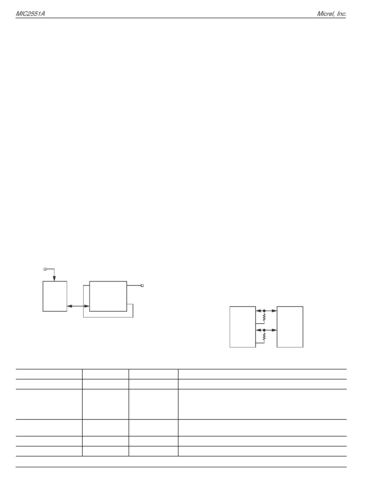
Non-Multiplexed Bus
In order to save pin count for the USB logic controller
interface, the MIC2551A was designed with VP and VM as bi-
directional pins. To interface the MIC2551A with a non-
multiplexed data bus, resistors can be used for low cost
isolation as shown in Figure 9.
USB Logic
Controller
(SIE)
MIC2551A
VP
VP
10k
VPO
VM
VM
10k
VMO
Figure 9. MIC2551A Interface to
Non-Multiplexed Data Bus
M9999-051004
8
May 2004
Share Link: 