MICRF103 查看數據表(PDF) - Micrel
零件编号
产品描述 (功能)
生产厂家
MICRF103 Datasheet PDF : 7 Pages
| |||
MICRF103
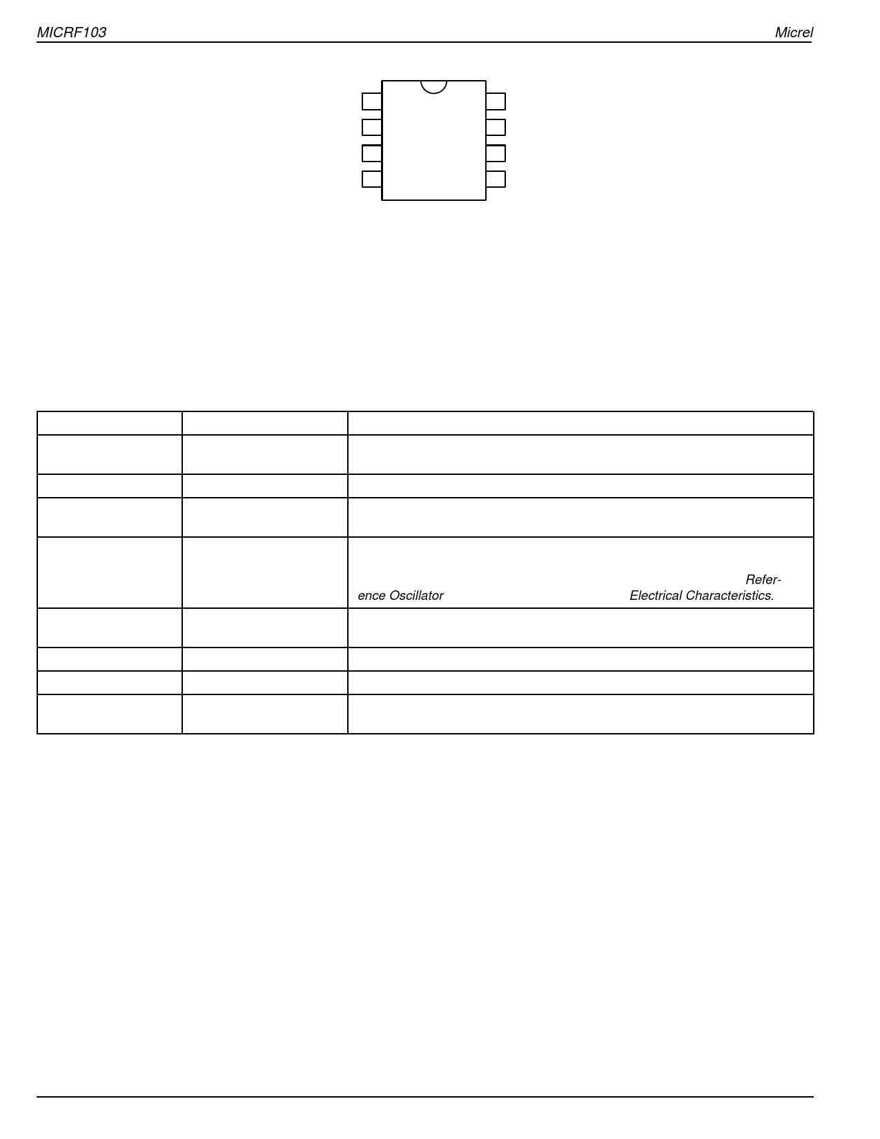
Pin Configuration
PC 1
VDD 2
VSS 3
REFOSC 4
8 ASK
7 ANTP
6 ANTM
5 STBY
MICRF103BM
Micrel
Pin Description
Pin Number
1
2
3
4
5
6
7
8
Pin Name
PC
VDD
VSS
REFOSC
STBY
ANTM
ANTP
ASK
Pin Function
Power Control Input. The voltage at this pin should be set between 0.1V to
0.4V for normal operation.
Positive power supply input for the IC.
This pin is the ground return for the IC. A power supply bypass capacitor
connected from VDD to VSS should have the shortest possible path.
This is the timing reference frequency which is the transmit frequency
divided by 64. Connect a crystal (mode dependent) between this pin and
VSS, or drive the input with an AC coupled 0.5Vpp input clock. See Refer-
ence Oscillator section in this data sheet under Electrical Characteristics.
Input for transmitter stand-by control pin is pulled to VDD for transmit
operation and VSS for stand-by mode.
Negative RF power output to drive one side of the transmit antenna.
Positive RF power output to drive the other side of the transmit antenna.
Amplitude Shift Key modulation data input pin. For CW operation, connect
this pin to VDD.
MICRF103
2
June 2002
Share Link: 