ML9041A-XXB 查看數據表(PDF) - Oki Electric Industry
零件编号
产品描述 (功能)
生产厂家
ML9041A-XXB Datasheet PDF : 64 Pages
| |||
OKI Semiconductor
PEDL9041A-02
ML9041A-xxA/xxB
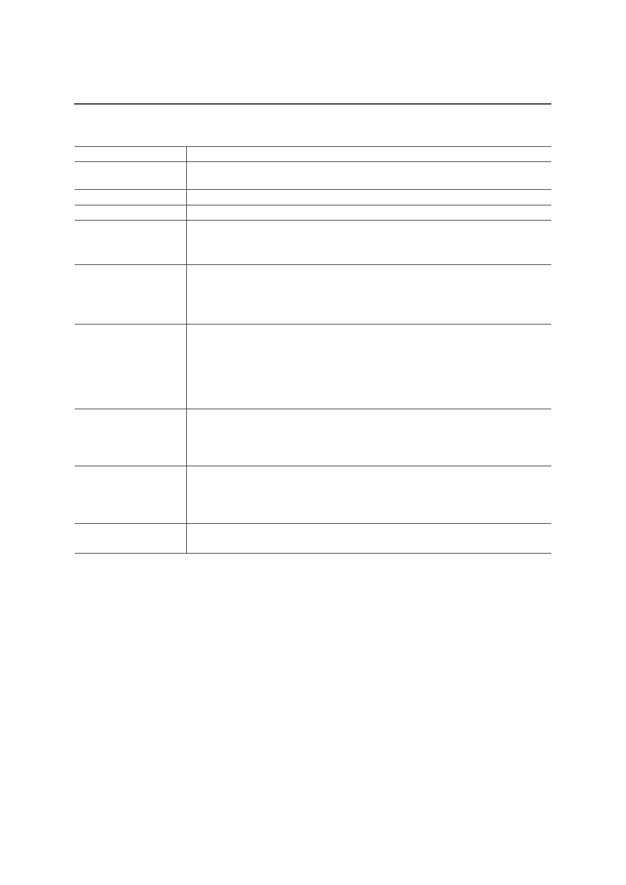
Symbol
T1, T2, T3
VDD
GND
S/P
CS
SHT
Sl
SO
DUMMY
Description
The input pins for test circuits (normally open). Each of these pins is equipped with a
pull-down resistor, so this pin should be left open.
The power supply pin.
The ground level input pin.
The input pin to select the serial or parallel interface.
“L” selects the parallel interface.
“H” selects the serial interface.
The pin to enable this IC in the serial l/F mode.
“L” enables this IC.
“H” disables this IC.
This pin should be open in the parallel l/F mode.
The pin to input shift clock in the serial l/F mode.
Data inputting to the SI pin is carried out synchronizing with the rising edge of this
clock signal.
Data outputting from the SO pin is carried out synchronizing with the falling edge of
this clock signal.
This pin should be open in the parallel l/F mode.
The pin to input DATA in the serial l/F mode.
Data inputting to this pin is carried out synchronizing with the rising edge of the SHT
signal.
This pin should be open in the parallel l/F mode.
The pin to output DATA in the serial l/F mode.
Data inputting to this pin is carried out synchronizing with the falling edge of the SHT
signal.
This pin should be open in the parallel l/F mode.
NC pin.
Leave this pin open.
6/64
Share Link: 