MLS9109-00881 查看數據表(PDF) - Tyco Electronics
零件编号
产品描述 (功能)
生产厂家
MLS9109-00881 Datasheet PDF : 2 Pages
| |||
Surface Mount Frequency Synthesizer
MLS9109-00881
MLS9109-00881
Surface Mount Frequency Synthesizer
CDMA 869 -894 MHz
Features
• Integrated VCO/PLL
• Miniature SMT Package
• Low Phase Noise
• +5V Operation
Description
The MLS9109-00881 synthesizer design integrates a high perfor-
mance buffered VCO, PLL circuit and discrete loop filter in a
surface mount package. The SMT packaging provides electrical
shielding, easy PCB assembly and repeatable performance. The
synthesizer is designed for use in CDMA base stations and is
optimised for coverage of the cellular Tx band, 30 kHz step size
and low phase noise requirements.
M/A-COM synthesizers are manufactured in an ISO 9001 certi-
fied facility, incorporating surface mount assembly and automated
electrical testing. This ensures consistent electrical performance
and quality over volume production quantities.
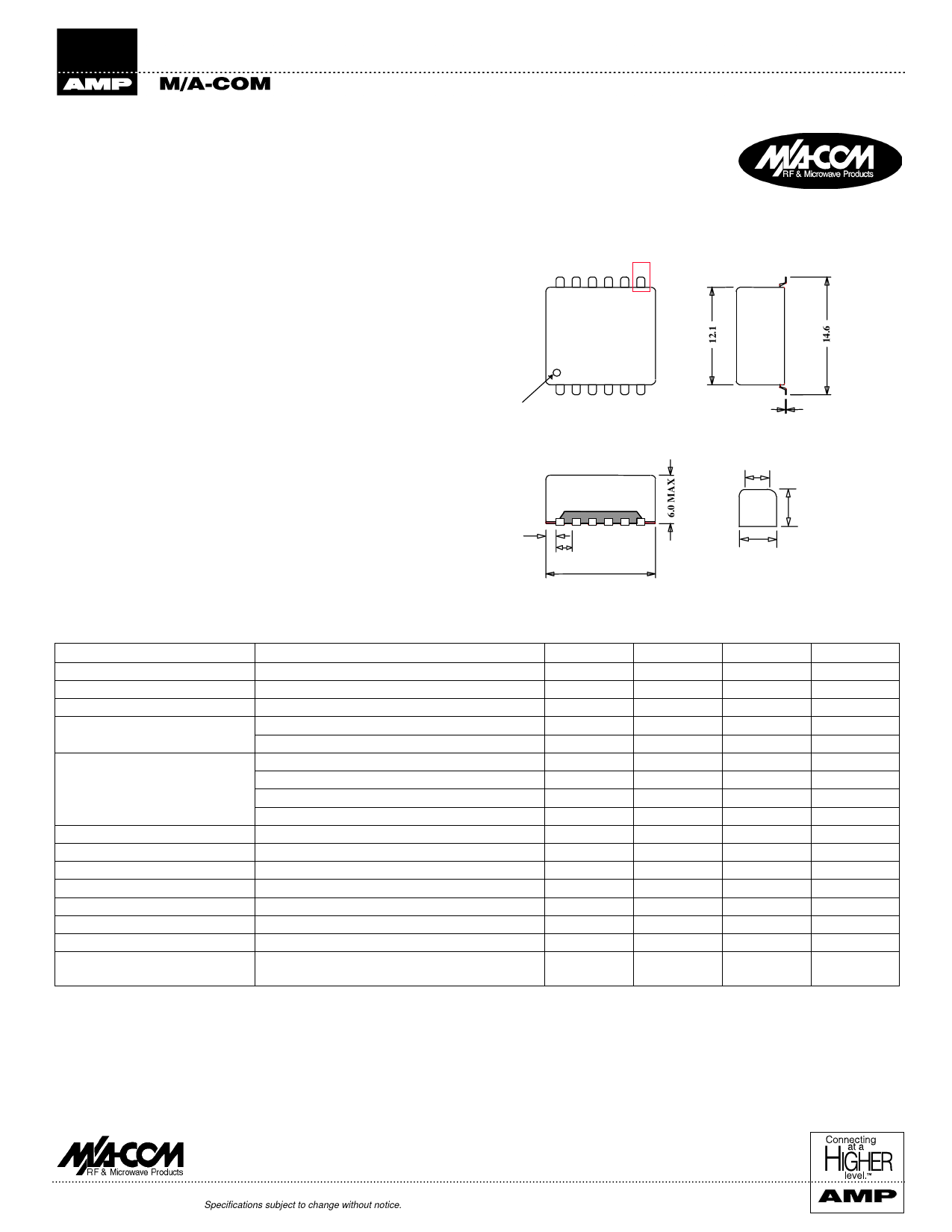
12 Lead Package
12 11 10 9 8 7 DETAIL A
M/ A- COM LTD
PART NO.
DATE CODE
12 34 5 6
IDENT
0.2
1.8
2.0
TYP. in 5 POSITIONS
13.6 MAX
0.6
0.8
1.0
DETAIL A
Electrical Specifications1, TA = +25°C, VCC = +5V , ∆F = 30 kHz, FR = 15 MHz (unless otherwise stated)
Parameter
Frequency Range (FOUT)2
RF Output Power (POUT)3
Harmonic Output
Spurious Output
Phase Noise4
Integrated Phase Noise
Frequency Switching Time5,6
VCO Supply Current (ICC1)
PLL Supply Current (ICC2)
VCO Supply Voltage (VCC1)
PLL Supply Voltage (VCC2)
Step Size (∆F)7
Reference Frequency (FR)8
Over TOP
Over TOP
Test Conditions
Phase comparison frequency (FOUT ± ∆F)
Reference breakthrough (FOUT ± FR)
SSB at 500 Hz offset from carrier
SSB at 1 kHz offset from carrier
SSB at 10 kHz offset from carrier
SSB at 100 kHz offset from carrier
300 Hz to 3 kHz bandwidth
Over FOUT, measured to within ± 500 Hz
Recommended operating limit
Recommended operating limit
Recommended operating limit
0.5 to 2.0 Vpp sine wave into a.c. coupled
CMOS. Recommended operating limit
Units
MHz
dBm
dBc
dBc
dBc
dBc/Hz
dBc/Hz
dBc/Hz
dBc/Hz
mrad rms
ms
mA
mA
V
V
kHz
MHz
Min.
869
-1.0
+4.75
+4.75
3
Typ.
-15
-85
-90
-70
-80
-107
-128
12
25
15
7
30
Max.
894
+5.0
-12
-70
-60
-75
-100
-120
20
12
+5.25
+5.25
20
1. All specification limits are indicated values and apply over FOUT and
for 50 Ω load impedance.
2. Programming control is 3 wire serial CMOS or TTL levels, in accor-
dance with National Semiconductor LMX 1511.
3. Output power window includes variation over operating temperature
range (TOP) -40°C to +85°C and output frequency range (FOUT).
4. See plot for typical phase noise at other frequency offsets.
5. See plot for typical full band switching time measured to within
other offsets from final frequency.
6. Integral PLL lock monitor output, TTL high locked, TTL low un-
locked.
7. Device designed for loop bandwidth of 150 Hz.
8. Reference frequency input impedance 10 kΩ min.
V2.00
www.macom.com
M/A-COM Division of AMP Incorporated s North America: Tel. (800) 366-2266, Fax (800) 618-8883 s Asia/Pacific: Tel.+85 2 2111 8088,
Fax +85 2 2111 8087 s Europe: Tel. +44 (1344) 869 595, Fax+44 (1344) 300 020
AMP and Connecting at a Higher Level are trademarks.
Specifications subject to change without notice.
Share Link: 