MN86157 查看數據表(PDF) - Panasonic Corporation
零件编号
产品描述 (功能)
生产厂家
MN86157 Datasheet PDF : 8 Pages
| |||
For Communications Equipment
MN86157
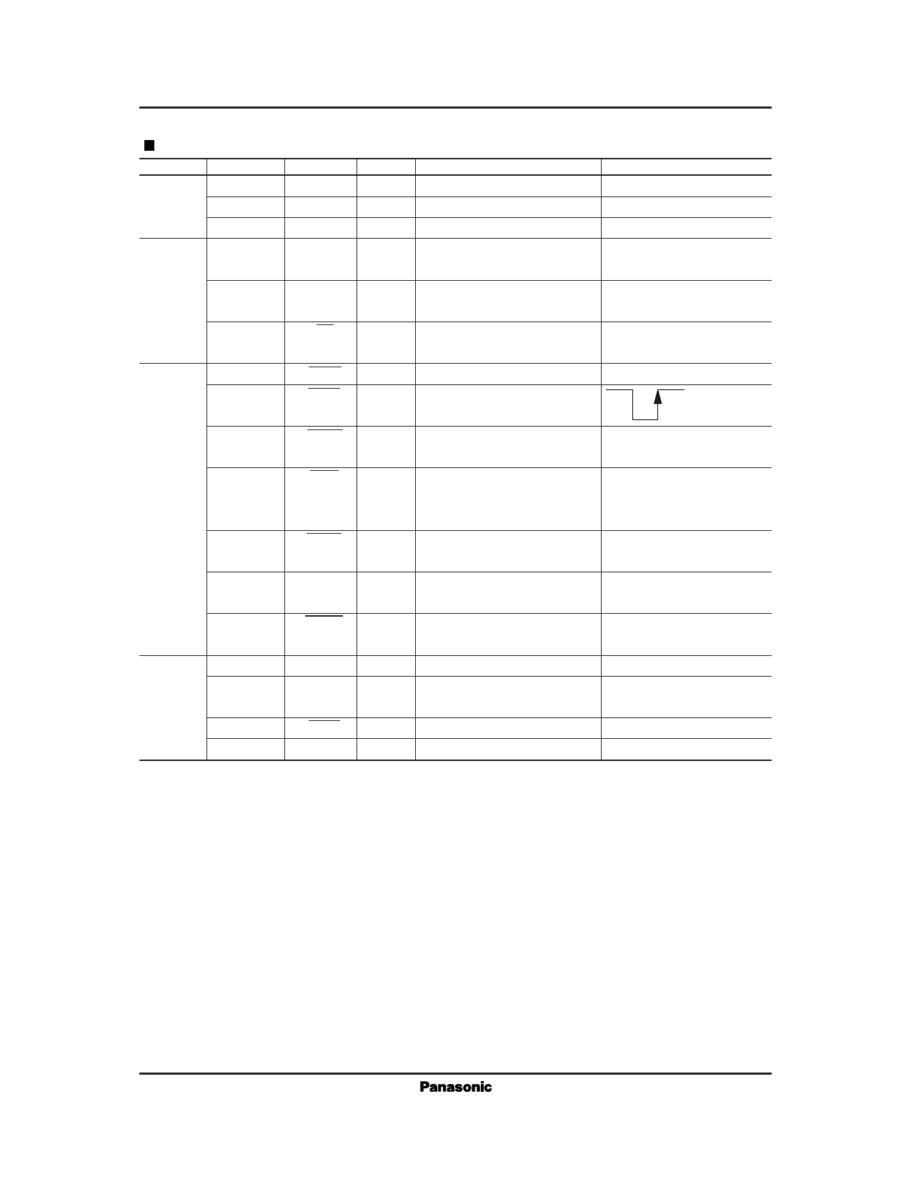
Pin Descriptions
Parameter Pin No.
A/D
15
converter
14
block
16
MULT
11 to 6
converter
block
5
12
CTL
23
converter
22
block
24
20
25
3
26
RAM
/ROM
IO
converter
block
39 to 28
40 to 44,
1, 2
21
4
Symbol I/O
VIN
I
VREFH —
VREFL —
DB 0 to 5 O
OVF/DB6 O
OE
I
ENBI
I
SHST
I
CKSH
I
INHI
I
ENBO
O
ROS
I
MODE
I
A 0 to 11 O
D 0 to 6 I/O
R/W
O
MOE
O
Function Description
Analog image signal input
Remarks
Reference voltage input
"H" level reference voltage input
Reference ground
"L" level reference voltage input
Corrected image signal output MODE: H
/A/D converter data output
/MODE: L
Corrected image signal overflow MODE: H
output/A/D converter data output /MODE: L
Output enable signal input
H: Pins are high-impedance;
for DB0 – DB5 and OVF
L: Pins provide output
Enable signal input for single line
Start input for reading white
Low pulse
reference signal
signals start.
Clock signal input
The frequency must be twice
that of the image clock.
Signal for suspending correction in H: Normal correction
the middle of a line and holding operation;
the output at the current value L: Stop and hold
Enable signal for corrected
image data output
Correction range selection
H: 50% correction;
L: 75% correction
Operating mode selection
H: Shading correction;
L: A/D conversion only
RAM/ROM address output
RAM/ROM data I/O
RAM read/write signal
RAM/ROM output enable signal
Share Link: 