MPC7448 查看數據表(PDF) - Freescale Semiconductor
零件编号
产品描述 (功能)
生产厂家
MPC7448 Datasheet PDF : 60 Pages
| |||
General Parameters
4 General Parameters
The following list summarizes the general parameters of the MPC7448:
Technology
Die size
Transistor count
Logic design
Packages
Core power supply
I/O power supply
90 nm CMOS SOI, nine-layer metal
8.0 mm × 7.3 mm
90 million
Mixed static and dynamic
Surface mount 360 ceramic ball grid array (HCTE)
Surface mount 360 ceramic land grid array (HCTE)
Surface mount 360 ceramic ball grid array with lead-free spheres (HCTE)
1.30 V
(1700 MHz device)
1.25 V
(1600 MHz device)
1.20 V
(1420 MHz device)
1.15 V
(1000 MHz device)
1.5 V, 1.8 V, or 2.5 V
5 Electrical and Thermal Characteristics
This section provides the AC and DC electrical specifications and thermal characteristics for the
MPC7448.
5.1 DC Electrical Characteristics
The tables in this section describe the MPC7448 DC electrical characteristics. Table 2 provides the
absolute maximum ratings. See Section 9.2, “Power Supply Design and Sequencing,” for power
sequencing requirements.
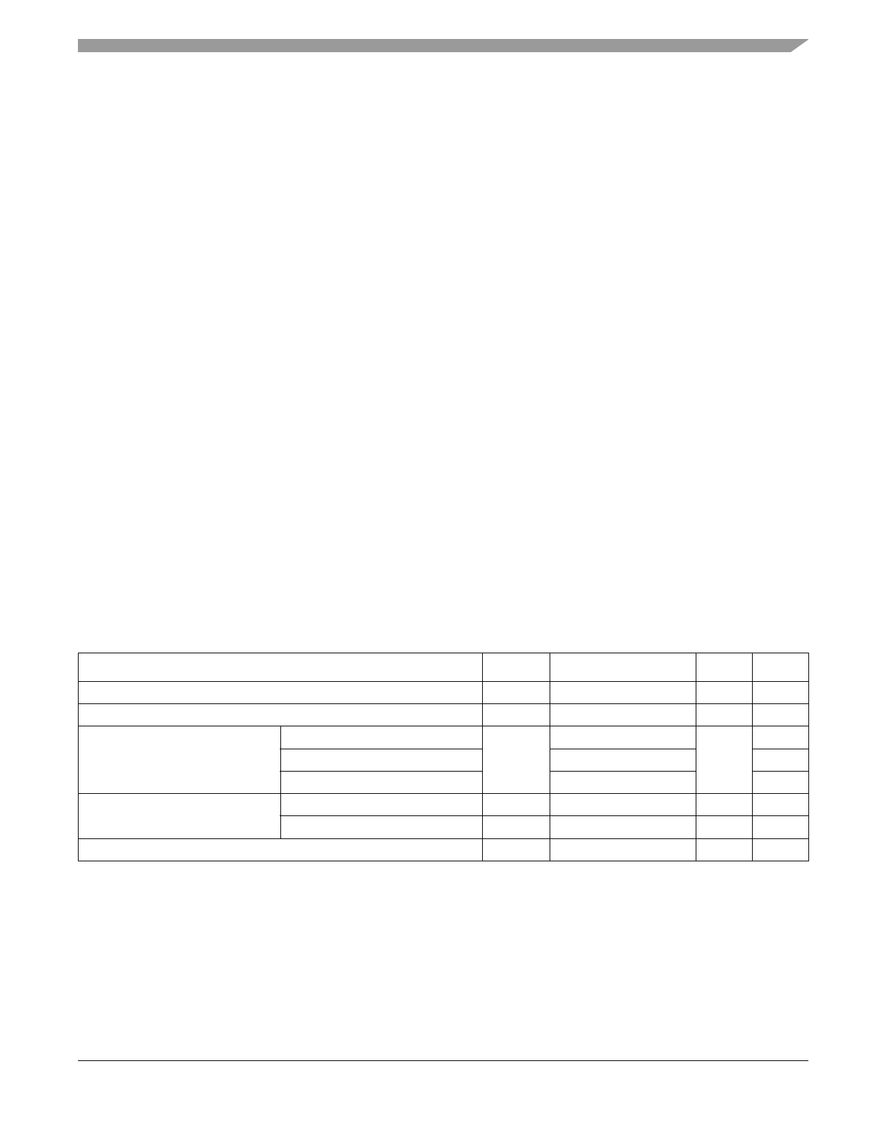
Table 2. Absolute Maximum Ratings 1
Characteristic
Symbol
Maximum Value
Unit Notes
Core supply voltage
PLL supply voltage
Processor bus supply voltage
I/O Voltage Mode = 1.5 V
I/O Voltage Mode = 1.8 V
VDD
AVDD
OVDD
–0.3 to 1.4
–0.3 to 1.4
–0.3 to 1.8
–0.3 to 2.2
V
2
V
2
V
3
3
I/O Voltage Mode = 2.5 V
–0.3 to 3.0
3
Input voltage
Processor bus
Vin
–0.3 to OVDD + 0.3
V
4
JTAG signals
Vin
–0.3 to OVDD + 0.3
V
Storage temperature range
Tstg
– 55 to 150
•C
Notes:
1. Functional and tested operating conditions are given in Table 4. Absolute maximum ratings are stress ratings only and
functional operation at the maximums is not guaranteed. Stresses beyond those listed may affect device reliability or cause
permanent damage to the device.
2. See Section 9.2, “Power Supply Design and Sequencing” for power sequencing requirements.
3. Bus must be configured in the corresponding I/O voltage mode; see Table 3.
4. Caution: Vin must not exceed OVDD by more than 0.3 V at any time including during power-on reset except as allowed by
the overshoot specifications. Vin may overshoot/undershoot to a voltage and for a maximum duration as shown in Figure 2.
MPC7448 RISC Microprocessor Hardware Specifications, Rev. 4
Freescale Semiconductor
9
Share Link: 