MPC7457(2004) 查看數據表(PDF) - Freescale Semiconductor
零件编号
产品描述 (功能)
生产厂家
MPC7457 Datasheet PDF : 68 Pages
| |||
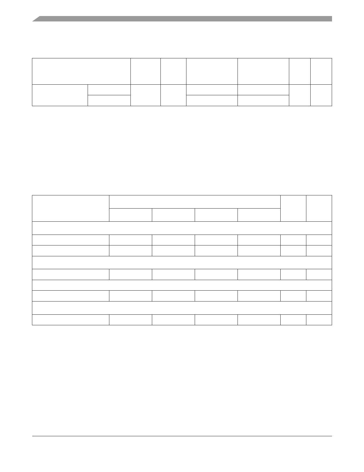
Electrical and Thermal Characteristics
Table 8. Clock AC Timing Specifications (continued)
At recommended operating conditions. See Table 4.
Maximum Processor Core Frequency
Characteristic
Symbol 867 MHz
1000 MHz
1200 MHz
1267 MHz Unit Notes
Min Max Min Max Min Max Min Max
SYSCLK cycle time
tSYSCLK 6.0
30
6.0
30
6.0
30
6.0
30
ns
2
SYSCLK rise and fall time
tKR, tKF —
1.0
—
1.0
—
1.0
—
1.0
ns
3
SYSCLK duty cycle measured tKHKL/
40
60
40
60
40
60
40
60
%
4
at OVDD/2
tSYSCLK
SYSCLK cycle-to-cycle jitter
— 150 — 150 — 150 — 150 ps
5, 6
Internal PLL relock time
— 100 — 100 — 100 — 100 µs
7
Notes:
1. Caution: The SYSCLK frequency and PLL_CFG[0:4] settings must be chosen such that the resulting SYSCLK (bus)
frequency, CPU (core) frequency, and PLL (VCO) frequency do not exceed their respective maximum or minimum operating
frequencies. Refer to the PLL_CFG[0:4] signal description in Section 1.9.1, “PLL Configuration,” for valid PLL_CFG[0:4]
settings.
2. Assumes lightly-loaded, single-processor system; see Section 5.2.1, “Clock AC Specifications” for more information.
3. Rise and fall times for the SYSCLK input measured from 0.4 to 1.4 V.
4. Timing is guaranteed by design and characterization.
5. Guaranteed by design.
6. The SYSCLK driver’s closed loop jitter bandwidth should be less than 1.5 MHz at –3 dB.
7. Relock timing is guaranteed by design and characterization. PLL-relock time is the maximum amount of time required for
PLL lock after a stable VDD and SYSCLK are reached during the power-on reset sequence. This specification also applies
when the PLL has been disabled and subsequently re-enabled during sleep mode. Also note that HRESET must be held
asserted for a minimum of 255 bus clocks after the PLL-relock time during the power-on reset sequence.
Figure 3 provides the SYSCLK input timing diagram.
SYSCLK
VM
VM
VM CVIL
CVIH
tKHKL
tKR
tKF
tSYSCLK
VM = Midpoint Voltage (OVDD/2)
Figure 3. SYSCLK Input Timing Diagram
5.2.2 Processor Bus AC Specifications
Table 9 provides the processor bus AC timing specifications for the MPC7457 as defined in Figure 4 and Figure 5.
Timing specifications for the L3 bus are provided in Section 5.2.3, “L3 Clock AC Specifications.”
MPC7457 RISC Microprocessor Hardware Specifications, Rev. 5
16
Freescale Semiconductor
Share Link: 