4226 查看數據表(PDF) - M.S. Kennedy Corporation
零件编号
产品描述 (功能)
生产厂家
4226 Datasheet PDF : 5 Pages
| |||
APPLICATION NOTES
MSK 4226 PIN DESCRIPTIONS
VCC - Is the low voltage supply for powering internal logic
and drivers for the lowside and highside MOSFETS.
The supplies for the highside drivers are derived from this
voltage.
V+ - Is the higher voltage H-bridge supply. The MOSFETS
obtain the drive current from this supply pin. The voltage on
this pin is limited by the drive IC. The MOSFETS are rated at
75 volts. Proper by-passing to GND with sufficient capaci-
tance to suppress any voltage transients, and to ensure re-
moving any drooping during switching, should be done as
close to the pins of the module as possible.
OUTPUT A - Is the output pin for one half of the bridge. De-
creasing the input voltage causes increasing duty cycles at
this output.
OUTPUT B - Is the output pin for the other half of the bridge.
Increasing the input voltage causes increasing duty cycles at
this output.
RSENSE A - Is the connection for the bottom of the A half
bridge. This can have a sense resistor connection to the V+
return ground for current limit sensing, or can be connected
directly to ground. The maximum voltage on this pin is ±2
volts with respect to GND.
RSENSE B - Is the connection for the bottom of the B half
bridge. This can have a sense resistor connection to the V+
return ground for current limit sensing, or can be connected
directly to ground. The maximum voltage on this pin is ±2
volts with respect to GND.
GND - Is the return connection for the input logic and Vcc.
DIS - Is the connection for disabling all 4 output switches.
DISABLE high overrides all other inputs. When taken low,
everything functions normally. An internal pullup to Vcc will
keep DISABLE high if left unconnected.
ALI - Is the logic level digital input for controlling the lowside
MOSFET in the A half bridge. If AHI is driven high or not
connected externally then ALI controls both the lowside and
highside MOSFETs, with dead time in between. This is due to
the simultaneous conduction lockout feature. DIS will over-
ride the ALI input.
AHI - Is the logic level digital input for controlling the highside
MOSFET in the A half bridge. ALI high level input will over-
ride this input to prevent simultaneous conduction. DIS will
override the AHI input.
BLI - Is the logic level digital input for controlling the lowside
MOSFET in the B half bridge. If BHI is driven high or not
connected externally then BLI controls both the lowside and
highside MOSFETs, with dead time in between. This is due to
the simultaneous conduction lockout feature. DIS will over-
ride the BLI input.
BHI - Is the logic level digital input for controlling the highside
MOSFET in the B half bridge. BLI high level input will override
this input to prevent simultaneous conduction. DIS will over-
ride the BHI input.
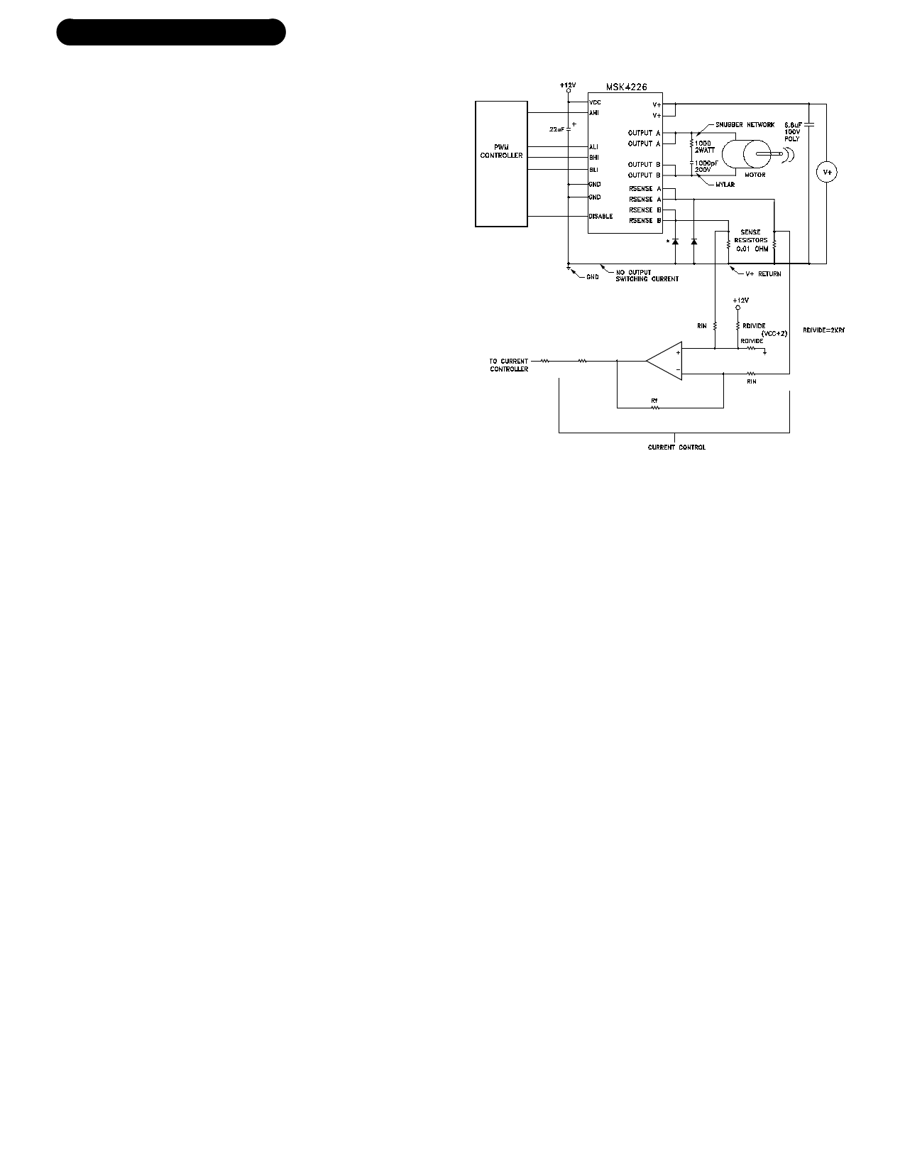
TYPICAL SYSTEM OPERATION
This is a diagram of a typical application of the MSK4226.
The design Vcc voltage is +12 volts and should have a good
low ESR bypass capacitor such as a tantalum electrolytic. The
digital inputs can come from a microprocessor or any type of
PWM controller. The controller will use the current sense
signal to either control current through PWM, current limit the
bridge, or both.
Current sensing is done in this case by a 0.01 ohm sense
IN resistor to sense current from both legs of the bridge sepa-
rately. It is important to make the high current traces as big as
possible to keep inductance down. The storage capacitor con-
nected to the V+ and the module should be large enough to
provide the high energy pulse without the voltage sagging
too far. A low ESR ceramic capacitor or large polypropylene
capacitor will be required. Mount the capacitor as close to the
module as possible. The connection between GND and the
V+ return should not be carrying any motor current. The
sense resistor signal is common mode filtered as necessary to
feed the limiting circuitry for the microprocessor. This appli-
cation will allow full four quadrant torque control for a closed
loop servo system. Any modulation scheme may be used,
however, but the current sensing scheme may have to change.
A snubber network is usually required, due to the induc-
tance in the power loop. It is important to design the snubber
network to suppress any positive spikes above 70V and nega-
tive spikes below -2V with respect to ground.
*There are certain inductive load situations that can possibly
cause a momentary shoot-through or cross-conduction condi-
tion in the MSK4226. This shoot-through is approximately
100nSec long and can be several amps, depending on the
layout and impedence of the bypassing circuit. Most bypass-
ing and current sensing filtering will usually eliminate the ef-
fects. However, in the case where it is still present, or the
sense resistor trace lengths are long, reverse-biased ultra-fast
recovery diodes or power schottky diodes from RSENSE A
and RSENSE B to power ground will minimize or eliminate the
situation.
3
Rev. B 11/04
Share Link: 