MSM6222 查看數據表(PDF) - Oki Electric Industry
零件编号
产品描述 (功能)
生产厂家
MSM6222
Oki Electric Industry

MSM6222 Datasheet PDF : 45 Pages
| |||
¡ Semiconductor
MSM6222B-xx
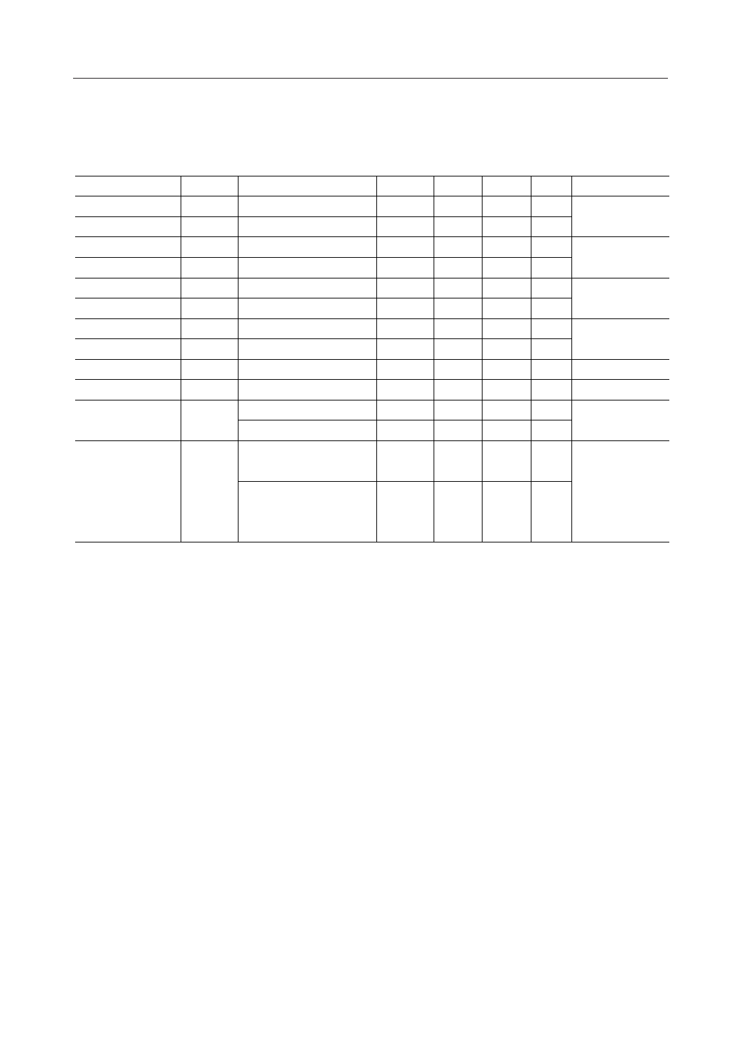
ELECTRICAL CHARACTERISTICS
DC Characteristics
Parameter Symbol
Condition
Min.
"H" Input Voltage
VIH1
"L" Input Voltage
VIL1
"H" Input Voltage
VIH2
"L" Input Voltage
VIL2
"H" Output Voltage VOH1
"L" Output Voltage VOL1
"H" Output Voltage VOH2
"L" Output Voltage VOL2
COM Voltage Drop VC
SEG Voltage Drop VS
Input Leakage Current IIL
—
—
—
—
IO = –0.205mA
IO = 1.2mA
IO = –40mA
IO = 40mA
IO = ±50mA
IO = ±50mA
VI = VSS
VI = VDD
VDD = 5.0V
VI = VSS
2.2
–0.3
VDD – 1.0
–0.3
2.4
—
0.9VDD
—
*1 —
*1 —
—
—
–50
Input Current
IIL2 VI = VDD, excluding current
flowing over pullup resistor —
and output drive MOS
(VDD = 4.5 to 5.5V, Ta = –20 to +75°C)
Typ. Max. Unit Applicable pin
—
VDD
V
R/W, RS, E,
—
0.6
V
DB0 - DB7
—
VDD
V
—
1.0
V
OSC1
—
—
V
—
0.4
V
DB0 - DB7
—
—
V
DO, CP, L,
— 0.1VDD V
DC, OSC2
—
2.9
V COM1 - COM16
—
3.8
V
SEG1 - SEG40
—
–1 mA
E
—
1
mA
–125 –250 mA
—
2
mA
R/W, RS
DB0 - DB7
*1 Applicable to the voltage drop (VC) occurring in pins VDD, V1, V4, and V5 to each COMMON
pin (COM1 to COM16) when 50 mA flows in or out of all COM and SEG pins. Also applicable
to voltage drop (VS) occurring in pins VDD, V2, V3, and V5 to each SEG pin (SEG1 to SEG40).
When output level is at VDD, V1 or V2 level, 50 mA flows out, while 50 mA flows in when the
output level is at V3, V4 or V5 level.
This occurs when +5V is input to VDD, V1, and V2, and when –3V is input to V3, V4, and V5.
7/45
Share Link: