MSM6262 查看數據表(PDF) - Oki Electric Industry
零件编号
产品描述 (功能)
生产厂家
MSM6262 Datasheet PDF : 52 Pages
| |||
¡ Semiconductor
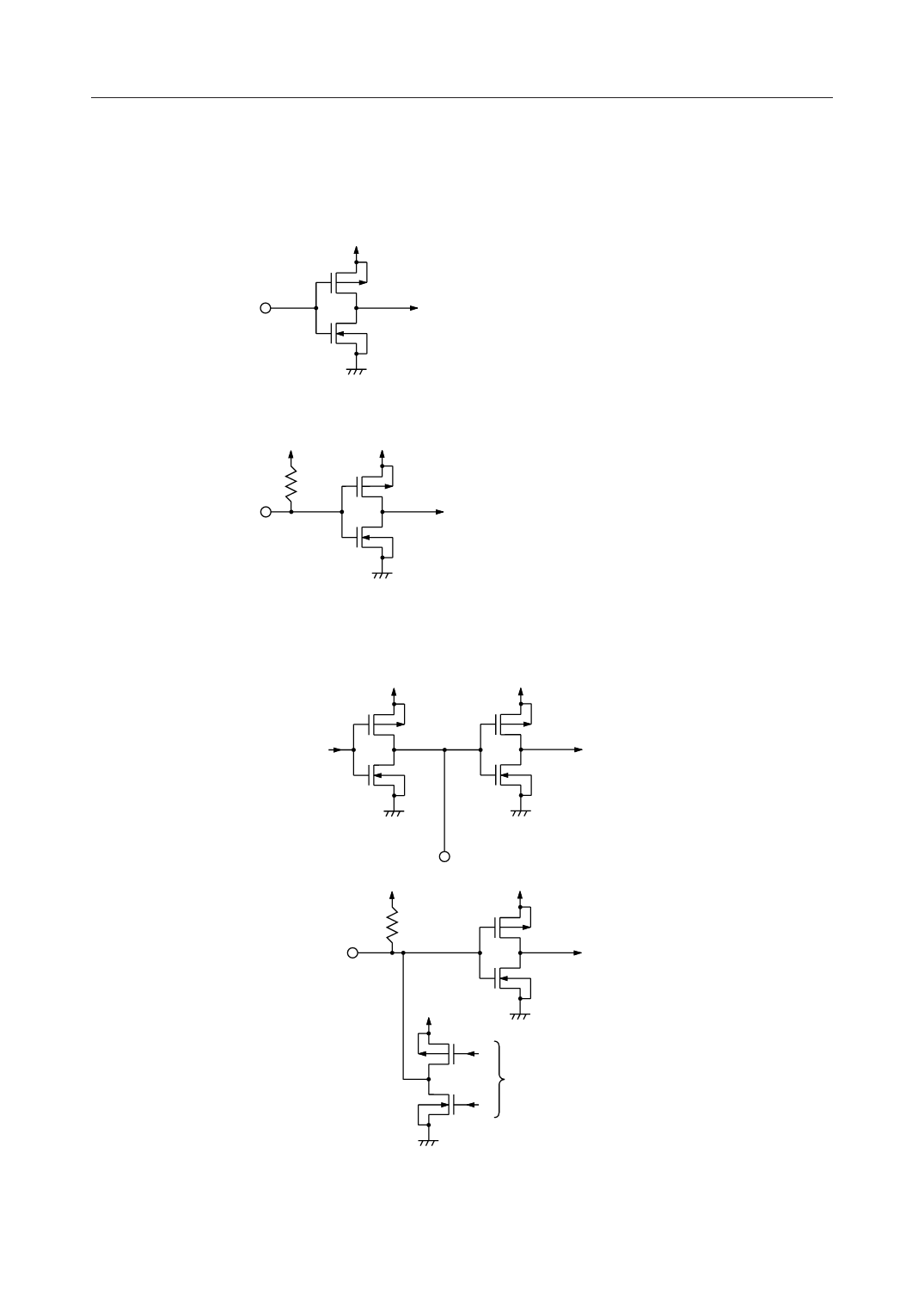
INPUT AND OUTPUT CONFIGURATION
Input pin
VDD
MSM6262-xx
To the inside of the device
Applicable pins: OSC1, 68 series/80 series, CS
R/W (WR), E (RD)
A0, A1
VDD
VDD
To the inside of the device
Applicable pin: RESET
Input /Output pin
VDD
VDD
From the inside of the device
To the inside of the device
Applicable pins:OSC2, OSC3
VDD
VDD
To the inside of of the device
VDD
From the inside of the device
Applicable pins: DB0 - DB7
3/52
Share Link: 