MSM6262 查看數據表(PDF) - Oki Electric Industry
零件编号
产品描述 (功能)
生产厂家
MSM6262 Datasheet PDF : 52 Pages
| |||
¡ Semiconductor
MSM6262-xx
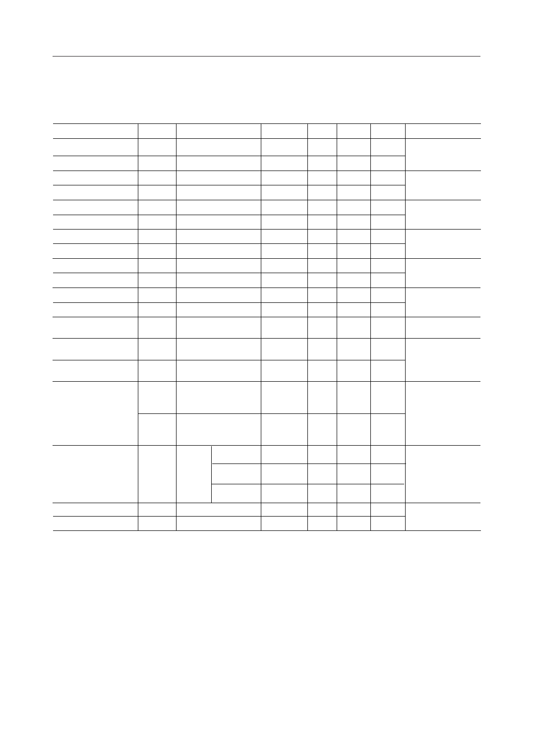
ELECTRICAL CHARACTERISTICS
DC Characteristics
Parameter Symbol
"H" Input Voltage
"L" Input Voltage
"H" Output Voltage
"L" Output Voltage
"H" Input Voltage
"L" Input Voltage
"H" Output Voltage
"L" Output Voltage
"H" Output Voltage
"L" Output Voltage
"H" Output Voltage
"L" Output Voltage
COM Voltage Drop
VIH1
VIL1
VOH1
VOL1
VIH2
VIL2
VOH2
VOL2
VOH3
VOL3
VOH4
VOL4
VCOM
"H" Input Current
IILH1
"L" Input Current
IILL1
IDD1
Supply Current
IDD2
Condition
––
––
IO = –250 mA
IO = 1.8 mA
––
––
IO = –500 mA
IO = 500 mA
IO = –1 mA
IO = 1 mA
IO = –100 mA
IO = 1.6 mA
IO = ± 50 mA *1
VIN = VDD
VIN = VSS
VDD = 5 V, *2
fOSC = 500 kHz
(RC oscillation)
VDD = 5 V,
*2
fIN = 500 kHz
(external oscillation)
Min.
2.2
–0.3
2.4
––
VDD–0.8
–0.3
0.85 VDD
––
0.85 VDD
––
2.4
––
(VDD = 4.5 to 5.5 V , Ta = –20 to +75°C)
Typ. Max.
–– VDD
–– 0.7
Unit
V
V
Applicable Pin
CS, R/W (WR)
E (RD), A0, A1
DB0 - DB7
–– ––
V
DB0 - DB7
–– 0.4
V
–– VDD
V
OSC1, RESET
–– 0.8
V
68series/80series
–– ––
V
–– 0.15 VDD V
DO, LOAD, DF
–– ––
V
CP
–– 0.15 VDD V
–– ––
V
BUSY1 OUT
–– 0.4
V
BUSY2 OUT
––
–– 2.9
V
COM1 - COM48
––
––
1
mA
CS, R/W (WR)
E (RD), A0, A1
––
––
–1
mA
OSC1, 68series/
80series
––
–– 1.5 mA
VDD
––
–– 1.5 mA
LCD Driving
Voltage
"H" Input Current
"L" Input Current
*3 1/5 bias
3.0
VLCD
VDD–V5
1/6-1/7
bias
4.0
1/8 bias
4.5
IILH2
VIN = VDD
––
IILL2
VIN = VSS,VDD = 5 V
–8
––
11
V
––
11
V
V1 , V4, V5
––
11
V
––
2
mA
RESET
–20 –60 mA
*1. This is applicable to the voltage drop which is caused between VDD, V1, V4, V5and COM1
- COM48 when a current of 50 mA is flowed in/out to/from all of COM1 - COM48. (When
the output level is either VDD or V1, it should be applied only when the current flows in.
When the output level is either V4 or V5, it should be applied only when the current flows
in.
In this case, +5V is applied to VDD and V1, while –6 V is applied to V4 and V5.)
*2. This is applicable to the current which flows in to VDD under following conditions.
VDD = 5 V, VSS = 0 V, V1 = 2.8 V, V4 = -3.8 V, V5 = –6 V, No load, No interface with CPU
*3. V1 to V5 should be set at as follows.
8/52
Share Link: 