MSM6575L 查看數據表(PDF) - Oki Electric Industry
零件编号
产品描述 (功能)
生产厂家
MSM6575L Datasheet PDF : 13 Pages
| |||
¡ Semiconductor
MSM6545/6575/6545L/6575L
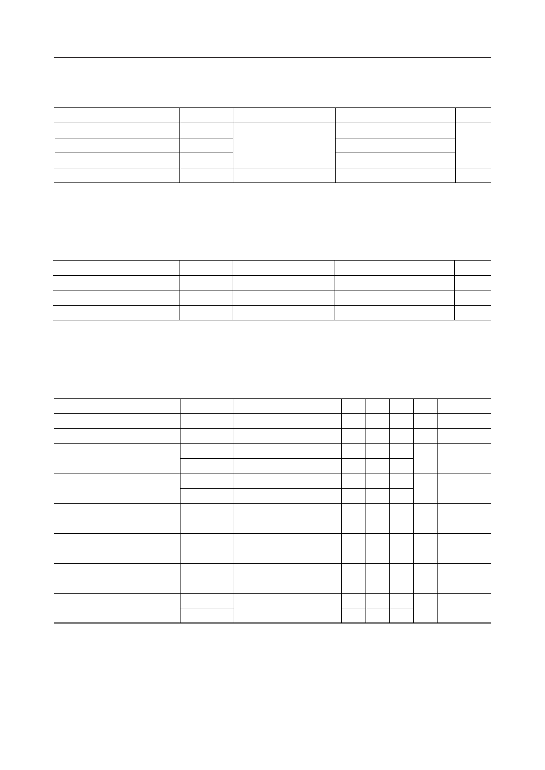
ABSOLUTE MAXIMUM RATINGS (MSM6545/6575, 1.5 V, BUF = "0")
Parameter
Symbol
Condition
VDD = 0 V (VSS1 = battery voltage)
Rating
Unit
Power Supply Voltage
Input Voltage
Output Voltage
Storage Temperature
VSS1
VIN
VOUT
TSTG
Ta = 25°C
—
–6.0 to +0.3
VSS1 – 0.3 to +0.3
V
VSS1 – 0.3 to +0.3
–55 to +125
°C
Note: The input of the constant voltage circuit is equal to the output of the voltage converter
(VSS2).
RECOMMENDED OPERATING CONDITIONS (MSM6545/6575, 1.5 V, BUF = "0")
Parameter
Symbol
Condition
VDD = 0 V (VSS1 = battery voltage)
Range
Unit
Operating Voltage
Vop
—
Operating Temperature
Top
—
Oscillation Frequency
fOSC
—
–1.75 to –0.9
V
–20 to +70
°C
32.768
kHz
Note: The input of the constant voltage circuit is equal to the output of the voltage converter
(VSS2).
ELECTRICAL CHARACTERISTICS (MSM6545/6575, 1.5 V, BUF = "0")
VDD = 0 V, VSS1 = –1.5 V (battery voltage), VSS2 = –3.0 V, fOSC = 32.768 kHz, CX = 35 pF, Ta = 25°C
Parameter
Symbol
Condition
Min. Typ. Max. Unit Applied Pin
Power Supply Current
Oscillation Start Voltage
Output Current 1
Output Current 2
Input Current 1
IDD
–VOSC
–IOH1
IOL1
–IOH2
IOL2
IIH1
*1
— 3 — mA
—
Within 2 seconds
VO = –0.5 V
VO = –1.0 V
VO = –0.5 V
VO = –1.0 V
— — 0.9 V
VSS1
150 — —
PORT0 to PORT6*2
mA
150 — —
SOUT, SCLK
20 — —
mA
BD
20 — —
VI = 0 V, in the input state, 7 15 30 mA PORT0 to
with pull-down resistor
PORT6 *2
Input Leakage Current
ÁIILÁ
VI = 0 V, –1.5 V, in the input state, — —
1
PORT0 to PORT7*2
mA
without pull-down resistor
SIN, SOUT, SCLK
Input Current 3
IIH3
VI = 0 V, with pull-down
resistor
RESET
70 250 500 mA
TEST1 to TEST3
Input Voltage
–VIH
— — 0.3
—
V All input pins
–VIL
1.2 — —
*1 Depends on the program. (Values in the above table are applied in the case where the
software duty is about 5%.)
*2 PORT0 = P0.0 to P0.3, PORT1 = P1.0 to P1.3, PORT2 = P2.0 to P2.3, PORT3 = P3.0 to P3.3,
PORT4 = P4.0 to P4.3, PORT5 = P5.0 to P5.3, PORT6 = P6.0 to P6.3, PORT7 = P7.0 to P7.3
Note: The input of the constant voltage circuit is equal to the output of the voltage converter
(VSS2).
5/13
Share Link: 