MSM6562B 查看數據表(PDF) - Oki Electric Industry
零件编号
产品描述 (功能)
生产厂家
MSM6562B Datasheet PDF : 50 Pages
| |||
¡ Semiconductor
MSM6562B-xx
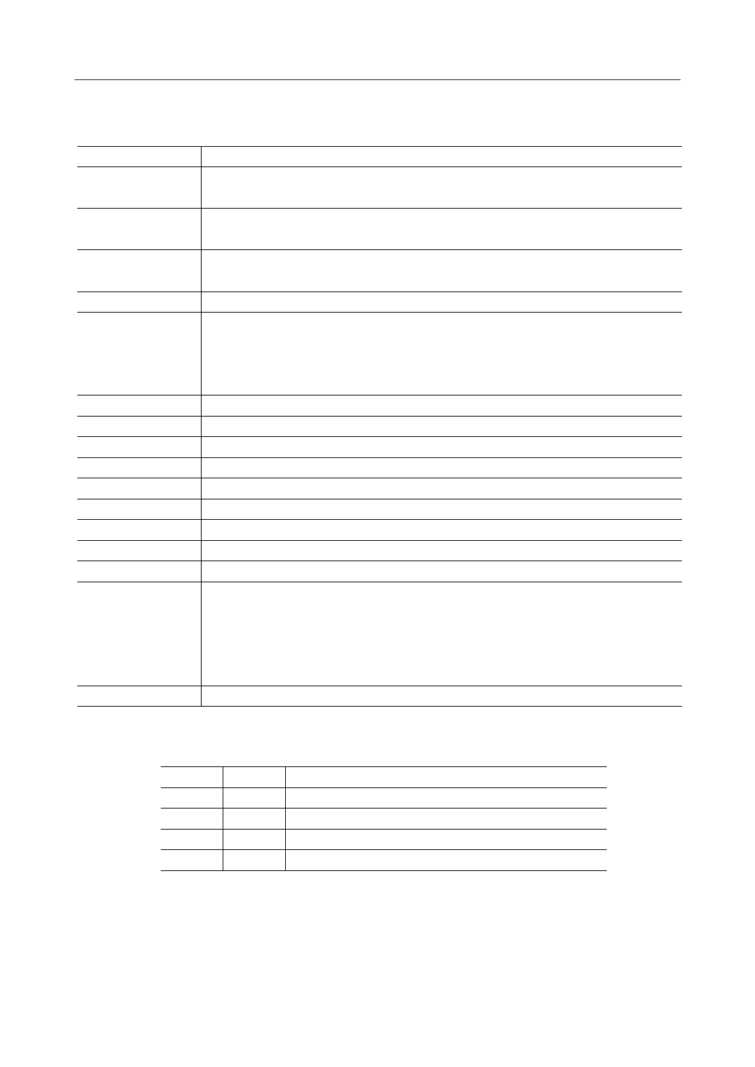
PIN DESCRIPTIONS
Symbol
R/W
RS0, RS1
E
DB0 - DB7
OSC1, OSC2,
OSCR
COM1 - COM16
SEG1 - SEG100
SHL0, SHL1
DO
CP
L
DF
VDD
VSS
V1 - V5, V3'
V5'
Description
Read/write selection input pin.
"H": Read, and "L": Write
Register selection input pins.
RS0 "H" RS1 "H": Data register
RS0 "L" RS1 "H" : Instruction register
RS0 "L" RS1 "L" : Contrast register
Input pin for data input/output between CPU and MSM6562B-xx and for activating
instruction.
Input/output pins for data send/receive between CPU and MSM6562B-xx.
Clock oscillating pins required for internal operation upon receipt of CPU instruction and
the LCD drive signal.
When oscillated by an external resistor, connect a resistor between OSC1 and OSC2.
When oscillated by a built-in resistor, connect OSCR and OSC2 externally.
LCD COMMON signal output pins.
LCD SEGMENT signal output pins.
Input pins to control the transfer direction of the SEGMENT signal output data. See table below.
Data output pin to send serial data to the character extension IC.
Clock output pin to transfer the serial data to the character extension IC.
Latch output pin to latch the transferred data to the character extension IC.
Output pin for the alternating signal (DF, display frequency) required for an LCD display.
Power supply pin.
Ground pin.
Bias voltage input pins to drive an LCD and bias setting pin. (Built-in bias dividing resistor)
1/4 bias : Connect V2 and V3. Leave V3' open.
1/5 bias : Connect V3 and V3'.
Since VLCD value depends on V5 voltage, connect a variable resistor between V5 pin and
VSS potential or connect V5 pin and V5' pin to adjust VLCD.
Contrast adjusting voltage output pin.
SHL0
L
L
H
H
SHL1
L
H
L
H
Segment data transfer direction
SEG1ÆSEG100
SEG100ÆSEG1
SEG1ÆSEG50fiSEG100ÆSEG51
SEG100ÆSEG1
4/50
Share Link: 