MSM6562B 查看數據表(PDF) - Oki Electric Industry
零件编号
产品描述 (功能)
生产厂家
MSM6562B Datasheet PDF : 50 Pages
| |||
¡ Semiconductor
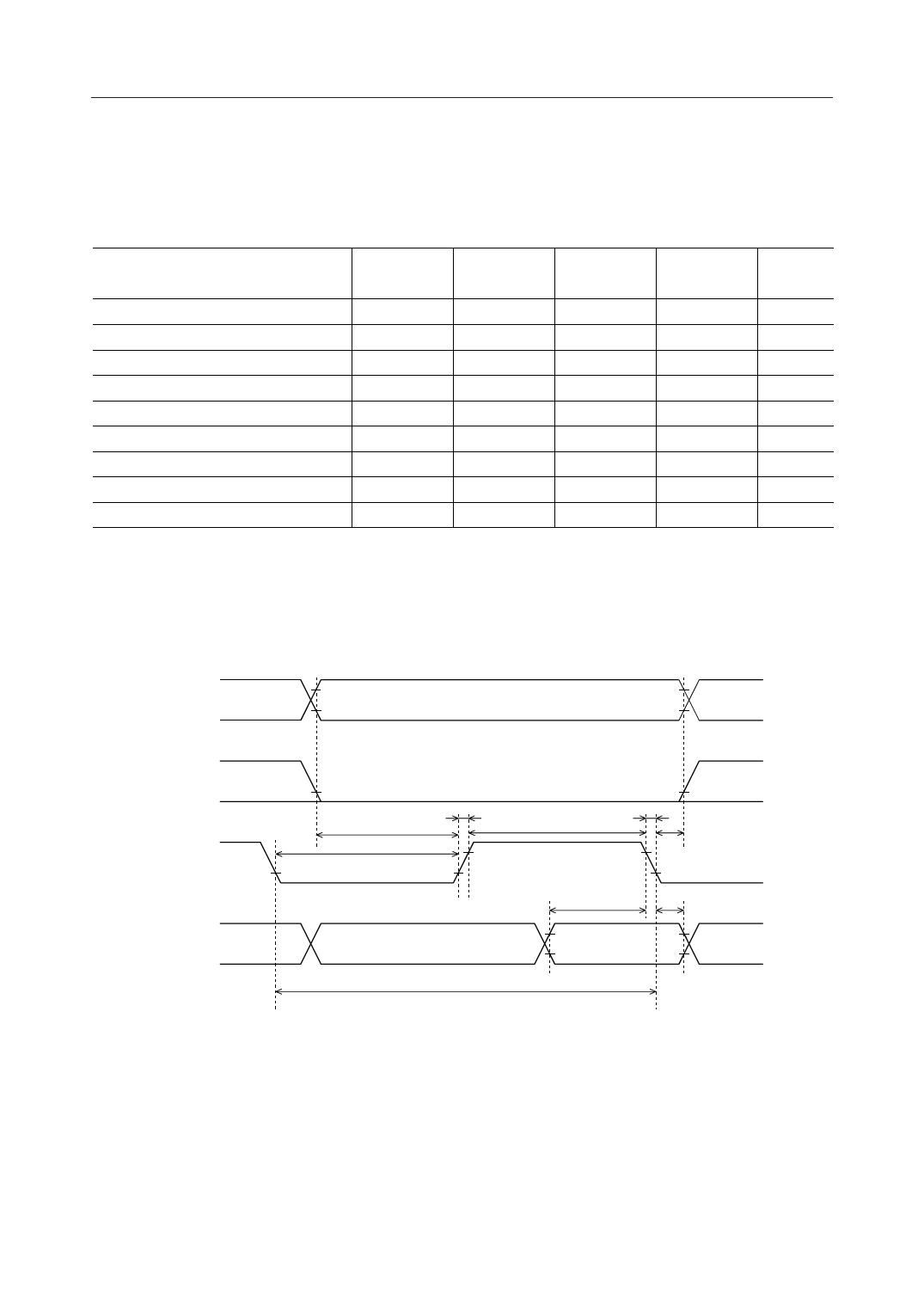
Switching Characteristics
1. Timing for input from the CPU (write operation)
Parameter
R/W, RS0 and RS1 setup time
E "H" pulse width
R/W, RS0 and RS1 hold time
E rise time
E fall time
E "L" pulse width
E cycle time
DB0 to DB7 input data setup time
DB0 to DB7 input data hold time
Symbol
tB
tW
tA
tr
tf
tL
tC
tI
tH
Min.
40
220
10
—
—
210
500
100
10
MSM6562B-xx
(VDD = 4.5 to 5.5V, Ta = –30 to +85°C)
Typ.
Max.
Unit
—
—
ns
—
—
ns
—
—
ns
—
20
ns
—
20
ns
—
—
ns
—
—
ns
—
—
ns
—
—
ns
RS1, 0
R/W
E
DB0-7
VIH1
VIL1
VIH1
VIL1
VIL1
tB
tL
VIL1
tr
VIH1
VIL1
tc
VIL1
tW
tf
tA
VIH1
VIL1
tI
tH
VIH1
VIL1
Input
data
VIH1
VIL1
9/50
Share Link: 