MSM80C85 查看數據表(PDF) - Oki Electric Industry
零件编号
产品描述 (功能)
生产厂家
MSM80C85 Datasheet PDF : 29 Pages
| |||
¡ Semiconductor
MSM80C85AHRS/GS/JS
BASIC SYSTEM TIMING
The MSM80C85AH has a multiplexed Data Bus. ALE is used as a strobe to sample the lower
8-bits of address on the Data Bus. Figure 5 shows an instruction fetch, memory read and I/O
write cycle (as would occur during processing of the OUT instruction). Note that during the I/
O write and read cycle that the I/O port address is copied on both the upper and lower half of
the address.
There are seven possible types of machine cycles. Which of these seven takes place is defined
by the status of the three status lines (IO/M, S1, S0) and the three control signals (RD, WR,and
INTA). (See Table 2.) The status line can be used as advanced controls (for device selection, for
example), since they become active at the T1 state, at the outset of each machine cycle. Control
lines RD and WR become active later, at the time when the transfer of data is to take place, so
are used as command lines.
A machine cycle normally consists of three T states, with the exception of OPCODE FETCH,
which normally has either four or six T states (unless WAIT or HOLD states are forced by the
receipt of READY or HOLD inputs). Any T state must be one of ten possible states, shown in
Table 3.
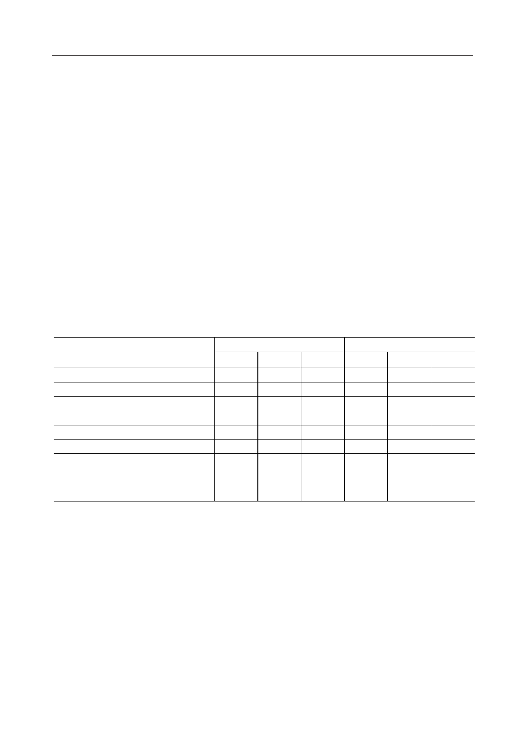
Table 2 MSM80C85AH Machine Cycle Chart
Machine Cycle
Status
IO/M
S1
S0
Opcode Fetch
(OF)
0
1
1
Memory Read
(MR)
O
1
O
Memory Write
(MW)
O
0
1
I/O Read
(IOR)
1
1
O
I/O Write
(IOW)
1
0
1
Acknowledge of INTR (INA)
1
1
1
Bus Idle
(BI): DAD
0
1
0
ACK. OF
RST, TRAP
1
1
1
HALT
TS
0
0
Control
RD
WR
0
1
O
1
1
0
O
1
1
0
1
1
1
1
1
1
TS
TS
INTA
1
1
1
1
1
0
1
1
1
9/29
Share Link: 