MT16VDDF12864HG-335 查看數據表(PDF) - Micron Technology
零件编号
产品描述 (功能)
生产厂家
MT16VDDF12864HG-335 Datasheet PDF : 31 Pages
| |||
512MB, 1GB (x64)
200-PIN DDR SODIMM
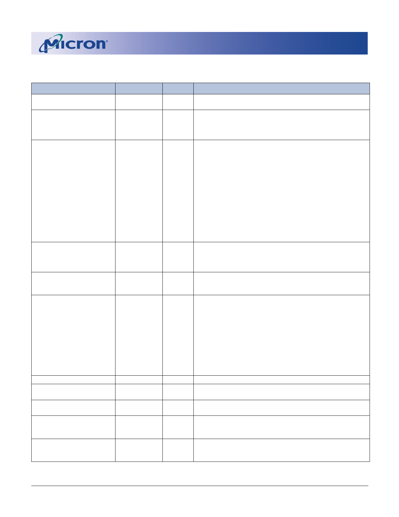
Table 5: Pin Descriptions
Pin numbers may not correlate with symbols. Refer to Pin Assignment Tables on page 3 for more information
PIN NUMBERS
118, 119, 120
35, 37, 158, 160
95, 96
SYMBOL
WE#,
CAS#,RAS#
CK0, CK0#
CK1, CK1#
CKE0, CKE1
121, 122
S0#, S1#
116, 117
BA0, BA1
99, 100, 101, 102, 105,106,
107, 108, 109, 110, 111, 112,
115
A0-A12
1, 2
195
194, 196, 198
193
VREF
SCL
SA0-SA2
SDA
12, 26, 48, 62, 134, 148, 170,
184
DM0-DM7
TYPE
Input
Input
Input
Input
Input
Input
Input
Input
Input
Input/
Output
Input
DESCRIPTION
Command Inputs: RAS#, CAS#, and WE# (along with S#) define
the command being entered.
Clock: CK, CK# are differential clock inputs. All address and
control input signals are sampled on the crossing of the
positive edge of CK, and negative edge of CK#. Output data
(DQs and DQS) is referenced to the crossings of CK and CK#.
Clock Enable: CKE HIGH activates and CKE LOW deactivates the
internal clock, input buffers and output drivers. Taking CKE
LOW provides PRECHARGE POWER-DOWN and SELF REFRESH
operations (all device banks idle), or ACTIVE POWER-DOWN
(row ACTIVE in any device bank). CKE is synchronous for
POWER-DOWN entry and exit, and for SELF REFRESH entry. CKE
is asynchronous for SELF REFRESH exit and for disabling the
outputs. CKE must be maintained HIGH throughout read and
write accesses. Input buffers (excluding CK, CK# and CKE) are
disabled during POWER-DOWN. Input buffers (excluding CKE)
are disabled during SELF REFRESH. CKE is an SSTL_2 input but
will detect an LVCMOS LOW level after VDD is applied and
until CKE is first brought HIGH. After CKE is brought HIGH, it
becomes an SSTL_2 input only.
Chip Selects: S# enables (registered LOW) and disables
(registered HIGH) the command decoder. All commands are
masked when S# is registered HIGH. S# is considered part of
the command code.
Bank Address: BA0 and BA1 define to which device bank an
ACTIVE, READ, WRITE, or PRECHARGE command is being
applied.
Address Inputs: Provide the row address for ACTIVE commands,
and the column address and auto precharge bit (A10) for
READ/WRITE commands, to select one location out of the
memory array in the respective device bank. A10 sampled
during a PRECHARGE command determines whether the
PRECHARGE applies to one device bank (A10 LOW, device bank
selected by BA0, BA1) or all device banks (A10 HIGH). The
address inputs also provide the op-code during a MODE
REGISTER SET command. BA0 and BA1 define which mode
register (mode register or extended mode register) is loaded
during the LOAD MODE REGISTER command.
SSTL_2 reference voltage.
Serial Clock for Presence-Detect: SCL is used to synchronize the
presence-detect data transfer to and from the module.
Presence-Detect Address Inputs: These pins are used to
configure the presence-detect device.
Serial Presence-Detect Data: SDA is a bidirectional pin used to
transfer addresses and data into and out of the presence-
detect portion of the module.
Data Write Mask. DM LOW allows WRITE operation. DM HIGH
blocks WRITE operation. DM lines do not affect READ
operation.
09005aef80a646bc
DDF16C64_128x64HG_B.fm - Rev. B 7/03 EN
4
Micron Technology, Inc., reserves the right to change products or specifications without notice.
©2003 Micron Technology, Inc.
Share Link: 