MT46V128M8 查看數據表(PDF) - Micron Technology
零件编号
产品描述 (功能)
生产厂家
MT46V128M8 Datasheet PDF : 74 Pages
| |||
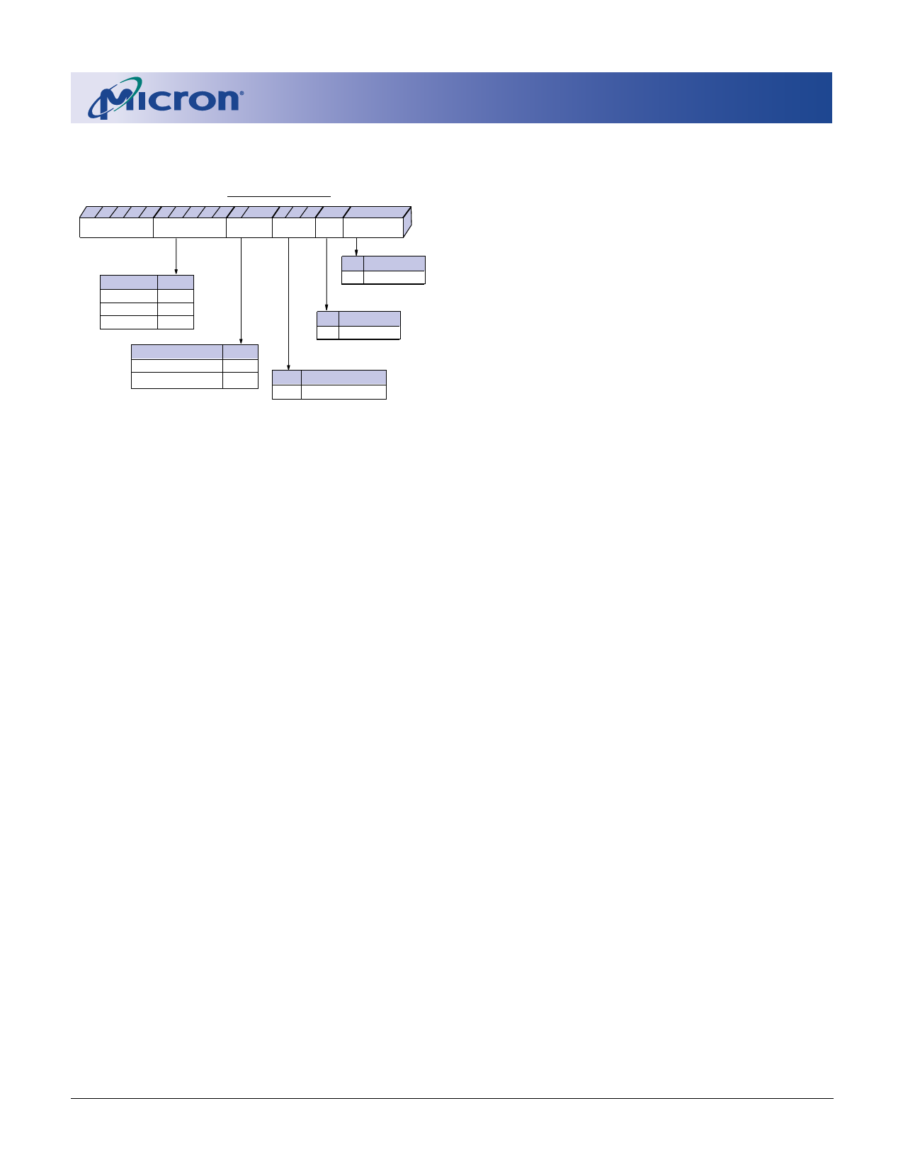
1Gb DDR SDRAM Part Numbers
Example Part Number: MT46V64M16TG-75
MT46V
Configuration
-
Package
Speed Special Temperature
Options
Configuration
256 Meg x4
128 Meg x8
64 Meg x16
256M4
128M8
64M16
Package
400 mil TSOP
TG
400 mil TSOP Lead-Free P
Operating Temp
Standard
Special Options
Standard
Speed Grade
-75 tCK=7.5ns, CL = 2.5
General Description
The 1Gb DDR SDRAM is a high-speed CMOS,
dynamic random-access memory containing
1,073,741,824 bits. It is internally configured as a quad-
bank DRAM.
The 1Gb DDR SDRAM uses a double data rate archi-
tecture to achieve high-speed operation. The double
data rate architecture is essentially a 2n-prefetch
architecture with an interface designed to transfer two
data words per clock cycle at the I/O pins. A single read
or write access for the 1Gb DDR SDRAM effectively
consists of a single 2n-bit wide, one-clock-cycle data
transfer at the internal DRAM core and two corre-
sponding n-bit wide, one-half-clock-cycle data trans-
fers at the I/O pins.
A bidirectional data strobe (DQS) is transmitted
externally, along with data, for use in data capture at
the receiver. DQS is a strobe transmitted by the DDR
SDRAM during READs and by the memory controller
during WRITEs. DQS is edge-aligned with data for
READs and center-aligned with data for WRITEs. The
x16 offering has two data strobes, one for the lower
byte and one for the upper byte.
The 1Gb DDR SDRAM operates from a differential
clock (CK and CK#); the crossing of CK going HIGH
and CK# going LOW will be referred to as the positive
edge of CK. Commands (address and control signals)
are registered at every positive edge of CK. Input data
is registered on both edges of DQS, and output data is
referenced to both edges of DQS, as well as to both
edges of CK.
PRELIMINARY
1Gb: x4, x8, x16
DDR SDRAM
Read and write accesses to the DDR SDRAM are
burst oriented; accesses start at a selected location and
continue for a programmed number of locations in a
programmed sequence. Accesses begin with the regis-
tration of an ACTIVE command, which is then fol-
lowed by a READ or WRITE command. The address
bits registered coincident with the ACTIVE command
are used to select the bank and row to be accessed. The
address bits registered coincident with the READ or
WRITE command are used to select the bank and the
starting column location for the burst access.
The DDR SDRAM provides for programmable READ
or WRITE burst lengths of 2, 4, or 8 locations. An auto
precharge function may be enabled to provide a self-
timed row precharge that is initiated at the end of the
burst access.
As with standard SDR SDRAMs, the pipelined,
multibank architecture of DDR SDRAMs allows for
concurrent operation, thereby providing high effective
bandwidth by hiding row precharge and activation
time.
An auto refresh mode is provided, along with a
power-saving power-down mode. All inputs are com-
patible with the JEDEC Standard for SSTL_2. All full
drive option outputs are SSTL_2, Class II compatible.
NOTE: 1. The functionality and the timing specifica-
tions discussed in this data sheet are for the
DLL-enabled mode of operation.
2. Throughout the data sheet, the various fig-
ures and text refer to DQs as “DQ.” The DQ
term is to be interpreted as any and all DQ
collectively, unless specifically stated other-
wise. Additionally, the x16 is divided into
two bytes, the lower byte and upper byte.
For the lower byte (DQ0 through DQ7) DM
refers to LDM and DQS refers to LDQS. For
the upper byte (DQ8 through DQ15) DM
refers to UDM and DQS refers to UDQS.
3. Complete functionality is described
throughout the document and any page or
diagram may have been simplified to con-
vey a topic and may not be inclusive of all
requirements.
4. Any specific requirement takes precedence
over a general statement.
09005aef8076894f
1gbBDDRx4x8x16_1.fm - Rev. A 3/03 EN
2
Micron Technology, Inc., reserves the right to change products or specifications without notice.
©2003 Micron Technology. Inc.
Share Link: 