MT88E39 查看數據表(PDF) - Zarlink Semiconductor Inc
零件编号
产品描述 (功能)
生产厂家
MT88E39 Datasheet PDF : 16 Pages
| |||
MT88E39
Data Sheet
Ringing, on the other hand, does not pose a problem as it is ignored by the carrier detector.
Crystal Oscillator
The MT88E39 uses either a 3.579545 MHz ceramic resonator or crystal oscillator as the master timing source.
The crystal specification is as follows:
Frequency:
3.579545 MHz
Frequency tolerance:
±0.2%(-40°C+85°C)
Resonance mode:
Parallel
Load capacitance:
18 pF
Maximum series resistance: 150 ohms
Maximum drive level (mW): 2 mW
e.g., CTS MP036S
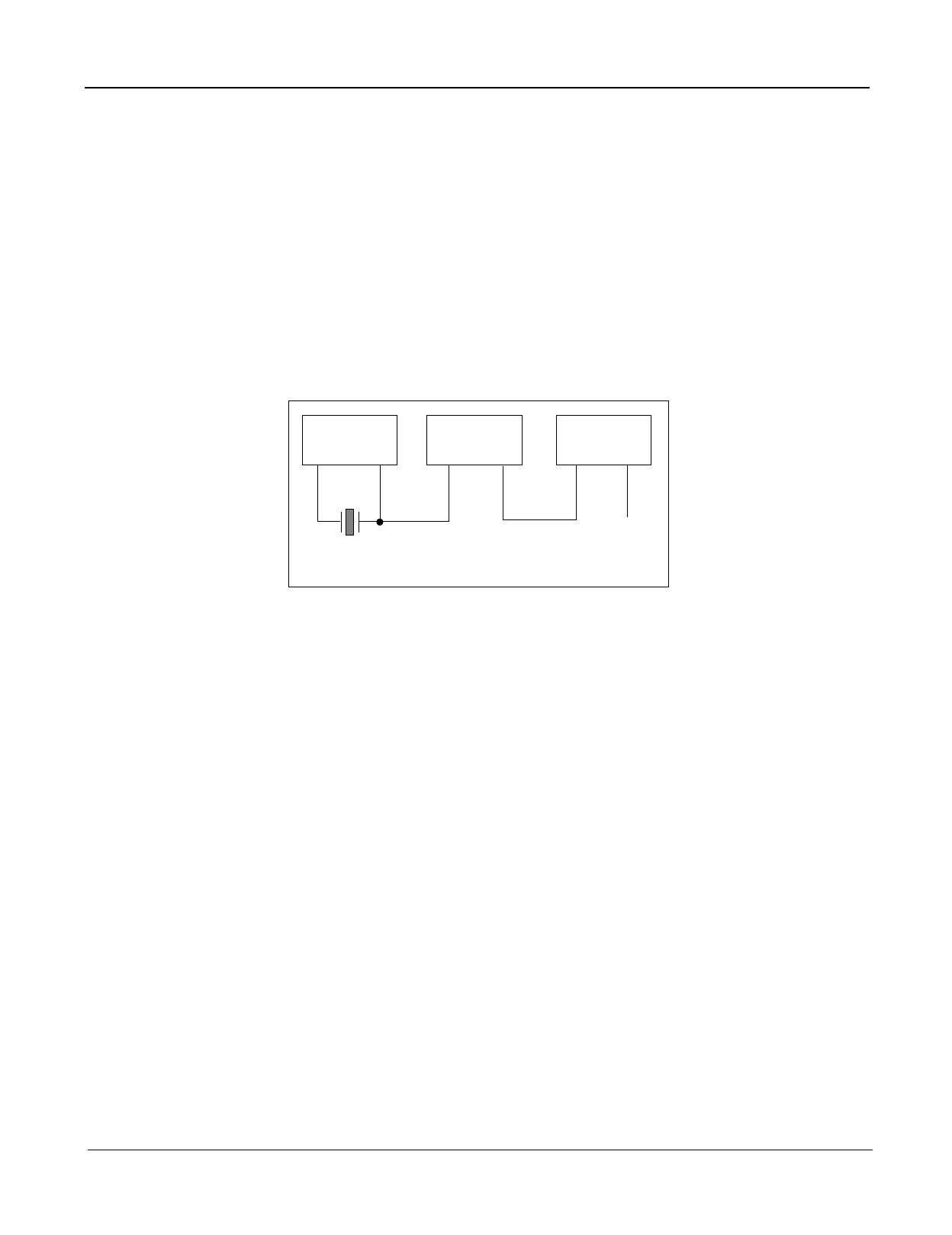
MT88E39
OSC1 OSC2
MT88E39
OSC1 OSC2
MT88E39
OSC1 OSC2
to the
3.579545 MHz
next MT88E39
(For 5 V application only)
Figure 5 - Common Crystal Connection
For 5 V applications any number of MT88E39 devices can be connected as shown in Figure 5 such that only one
crystal is required. The connection between OSC2 and OSC1 can be DC coupled as shown, or the OSC1 input on
all devices can be driven from a CMOS buffer (dc coupled) with the OSC2 outputs left unconnected.
VRef and CAP Inputs
VRef is the output of a low impedance voltage source equal to VDD/2 and is used to bias the input op-amp. A 0.1 µF
capacitor is required between CAP and VSS to suppress noise on VRef.
Applications
Table 1 shows the Bellcore and ETSI FSK signal characteristics. The application circuit in Figure 6 will meet these
requirements.
For 5 V designs the input op-amp should be set to unity gain to meet the Bellcore requirements and -2.5 dB gain for
ETSI requirements.
As supply voltage (VDD) is decreased, the FSK detect threshold will be lowered. Therefore for designs operating at
other than 5 V nominal voltage, to meet the FSK reject level requirement the gain of the op-amp should be reduced
accordingly.
For 3 V designs the gain settings for Bellcore and ETSI should be -3 dB and -5.5 dB respectively.
For applications requiring detection of lower FSK signal level, the input op-amp may be configured to provide
adequate gain. However, too much gain will cause noise tolerance to fail the TIA requirements because the FSK
signal will be clipped at GS when the single tone noise is added.
6
Zarlink Semiconductor Inc.
Share Link: 