MT9046(2003) 查看數據表(PDF) - Zarlink Semiconductor Inc
零件编号
产品描述 (功能)
生产厂家
MT9046 Datasheet PDF : 34 Pages
| |||
MT9046
Data Sheet
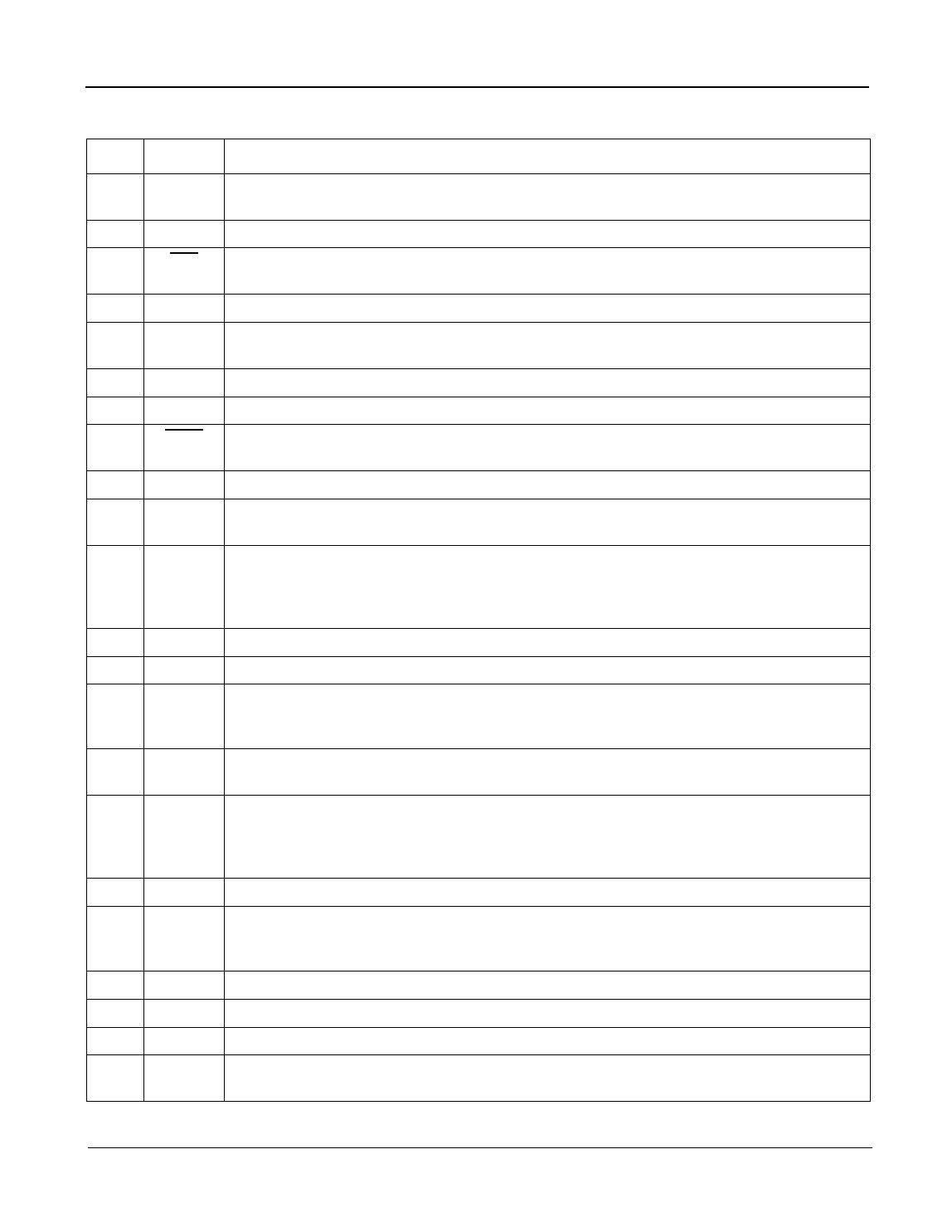
Pin Description (continued)
Pin #
33,34
36
37
38
39
40
41
42
43
44
45
46
47
48
Name
IC
MS2
MS1
RSEL
IC
FS2
FS1
IC
NC
TDO
TDI
TRST
TCK
TMS
Description
Internal Connection. Tie low for normal operation.
Mode/Control Select 2 (Input). This input determines the state (Normal, Holdover or
Freerun) of operation. The logic level at this input is gated in by the rising edge of F8o. See
Table 3.
Mode/Control Select 1 (Input). The logic level at this input is gated in by the rising edge of
F8o. See pin description for MS2. This pin is internally pulled down to VSS.
Reference Source Select (Input). A logic low selects the PRI (primary) reference source as
the input reference signal and a logic high selects the SEC (secondary) input. The logic level
at this input is gated in by the rising edge of F8o. See Table 2. This pin is internally pulled
down to VSS.
Internal Connection. Tie low for normal operation.
Frequency Select 2 (Input). This input, in conjunction with FS1, selects which of four
possible frequencies (8kHz, 1.544MHz, 2.048MHz or 19.44MHz) may be input to the PRI and
SEC inputs. See Table 1.
Frequency Select 1 (Input). See pin description for FS2.
Internal Connection. Tie low for normal operation.
No Connection. Leave open Circuit
Test Serial Data Out (CMOS Output). JTAG serial data is output on this pin on the falling
edge of TCK. This pin is held in high impedance state when JTAG scan is not enable.
Test Serial Data In (Input). JTAG serial test instructions and data are shifted in on this pin.
This pin is internally pulled up to VDD.
Test Reset (Input). Asynchronously initializes the JTAG TAP controller by putting it in the
Test-Logic-Reset state. If not used, this pin should be held low.
Test Clock (Input): Provides the clock to the JTAG test logic. This pin is internally pulled up to
VDD.
Test Mode Select (Input). JTAG signal that controls the state transitions of the TAP
controller. This pin is internally pulled up to VDD.
Functional Description
The MT9046 is a Multitrunk System Synchronizer with frequency holdover capability, providing timing (clock)
and synchronization (frame) signals to interface circuits for T1 and E1 Primary Rate Digital Transmission links.
Figure 1 is a functional block diagram which is described in the following sections.
Reference Select MUX Circuit
The MT9046 accepts two simultaneous reference input signals and operates on their falling edges. Either the
primary reference (PRI) signal or the secondary reference (SEC) signal can be selected as input to the TIE
Corrector Circuit. The selection is based on the Control, Mode and Reference Selection of the device. See
Table 1 and Table 4.
4
Zarlink Semiconductor Inc.
Share Link: 