CY7C1334 查看數據表(PDF) - Cypress Semiconductor
零件编号
产品描述 (功能)
生产厂家
CY7C1334 Datasheet PDF : 12 Pages
| |||
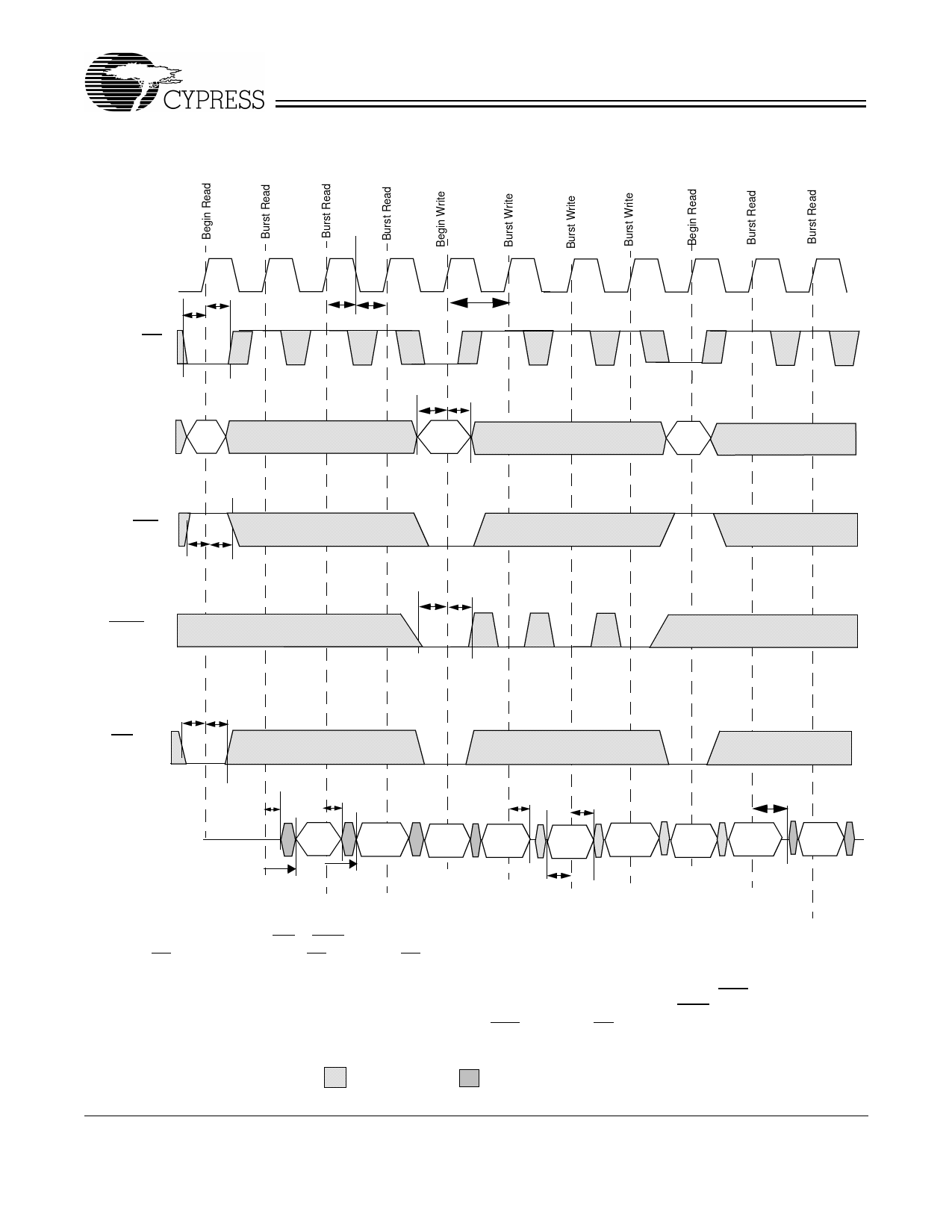
Switching Waveforms (continued)
Burst Sequences
CY7C1334
CLK
tALS
tALH
ADV/LD
tCH tCL
tCYC
ADDRESS RA1
tAS tAH
WA2
RA3
WE
tWS tWH
BWS[3:0]
tWS tWH
tCES tCEH
CE
tCLZ
tDOH
tCHZ
tDH
tCLZ
Data-
In/Out
Device
OQu11t a
Q1+1
Out
Q1+2 Q1+3
Out Out
D2
D2+1 D2+2 D2+3
Q3
In
In
In
In
Out
originally
deselected tCO
tCO
tDS
The combination of WE & BWS[3:0] define a write cycle (see Write Cycle Description table).
CE is the combination of CE1, CE2, and CE3. All chip enables need to be active in order to select
the device. Any chip enable can deselect the device. RAx stands for Read Address X, WA stands for
Write Address X, Dx stands for Data-in for location X, Qx stands for Data-out for location X. CEN held
LOW. During burst writes, byte writes can be conducted by asserting the appropriate BWS[3:0] input signals.
Burst order determined by the state of the Mode input. CEN held LOW. OE held LOW.
= DON’T CARE = UNDEFINED
Document #: 38-05065 Rev. **
Page 10 of 12
Share Link: 