CY7C1334 查看數據表(PDF) - Cypress Semiconductor
零件编号
产品描述 (功能)
生产厂家
CY7C1334 Datasheet PDF : 12 Pages
| |||
334
CY7C1334
64Kx32 Pipelined SRAM with NoBL™ Architecture
Features
• Pin compatible and functionally equivalent to ZBT™
device MT55L64L32P
• Supports 133-MHz bus operations with zero wait states
— Data is transferred on every clock
• Internally self-timed output buffer control to eliminate
the need to use OE
• Fully registered (inputs and outputs) for pipelined
operation
• Byte Write Capability
• 64K x 32 common I/O architecture
• Single 3.3V power supply
• Fast clock-to-output times
— 4.2 ns (for 133-MHz device)
— 5.0 ns (for 100-MHz device)
— 7.0 ns (for 80-MHz device)
— 10.0 ns (for 50-MHz device)
• Clock Enable (CEN) pin to suspend operation
• Synchronous self-timed writes
• Asynchronous output enable
• JEDEC-standard 100-pin TQFP package
• Burst Capability—linear or interleaved burst order
• Low (16.5 mW) standby power
Functional Description
The CY7C1334 is a 3.3V, 64K by 32 synchronous-pipelined
Burst SRAM designed specifically to support unlimited true
back-to-back Read/Write operations without the insertion of
wait states. The CY7C1334 is equipped with the advanced No
Bus Latency™ (NoBL™) logic required to enable consecutive
Read/Write operations with data being transferred on every
clock cycle. This feature dramatically improves the throughput
of the SRAM, especially in systems that require frequent
Write-Read transitions.The CY7C1334 is pin/functionally com-
patible to ZBT SRAM MT55L64L32P
All synchronous inputs pass through input registers controlled
by the rising edge of the clock. All data outputs pass through
output registers controlled by the rising edge of the clock. The
clock input is qualified by the Clock Enable (CEN) signal, which
when deasserted suspends operation and extends the previ-
ous clock cycle. Maximum access delay from the clock rise is
4.2 ns (133-MHz device).
Write operations are controlled by the four Byte Write Selects
(BWS[0-3]) and a Write Enable (WE) input. All writes are con-
ducted with on-chip synchronous self-timed write circuitry.
Three synchronous Chip Enables (CE1, CE2, CE3) and an
asynchronous Output Enable (OE) provide for easy bank se-
lection and output three-state control. In order to avoid bus
contention, the output drivers are synchronously three-stated
during the data portion of a write sequence.
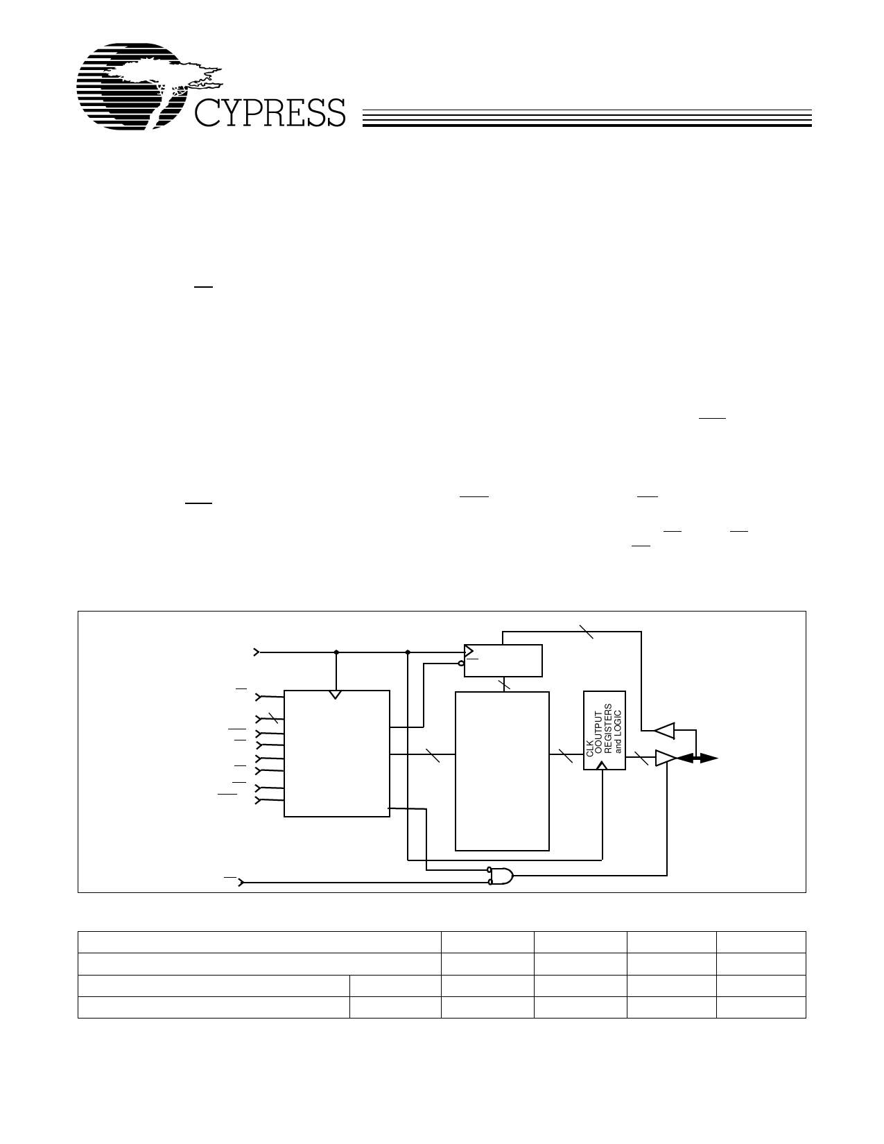
Logic Block Diagram
CLK
ADV/LD
16
A[15:0]
CEN
CE1
CE 2
CE 3
WE
BWS[3:0]
CONTROL
and WRITE
LOGIC
D
32
Data-In REG.
CE
Q
32
64KX32 32
MEMORY
16
ARRAY
32
DQ[31:0]
OE
.
Selection Guide
7C1334-133
Maximum Access Time (ns)
4.2
Maximum Operating Current (mA)
Commercial
400
Maximum CMOS Standby Current (mA)
Commercial
5.0
No Bus Latency and NoBL are trademarks of Cypress Semiconductor.
ZBT is a trademark of Integrated Device Technology.
7C1334-100
5.0
360
5.0
7C1334-80
7.0
310
5.0
7C1334-50
10
260
5.0
Cypress Semiconductor Corporation • 3901 North First Street • San Jose • CA 95134 • 408-943-2600
Document #: 38-05065 Rev. **
Revised August 20, 2001
Share Link: 