CY7C1334 查看數據表(PDF) - Cypress Semiconductor
零件编号
产品描述 (功能)
生产厂家
CY7C1334 Datasheet PDF : 12 Pages
| |||
CY7C1334
Burst Write Accesses
The CY7C1334 has an on-chip burst counter that allows the
user the ability to supply a single address and conduct up to
four Write operations without reasserting the address inputs.
ADV/LD must be driven LOW in order to load the initial ad-
dress, as described in the Single Write Access section above.
When ADV/LD is driven HIGH on the subsequent clock rise,
the chip enables (CE1, CE2, and CE3) and WE inputs are ig-
nored and the burst counter is incremented. The correct
BWS[3:0] inputs must be driven in each cycle of the burst write
in order to write the correct bytes of data.
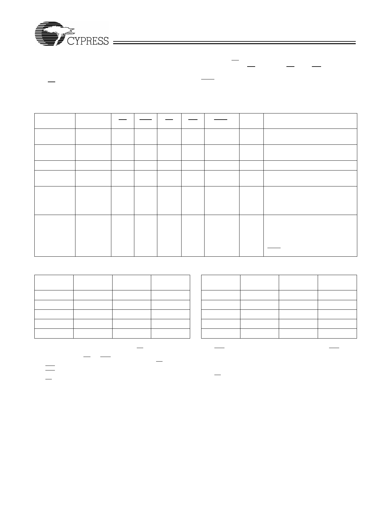
Cycle Description Truth Table[1, 2, 3, 4, 6, 7]
Address
ADV/
Operation
Used
CE CEN
LD
WE
Deselected External
1
0
L
X
Suspend
-
X
1
X
X
Begin Read External
0
0
0
1
Begin Write External
0
0
0
0
Burst Read
Operation
Internal
X
0
1
X
Burst Write
Operation
Internal
X
0
1
X
BWSx
X
X
X
Valid
X
Valid
CLK
L-H
L-H
L-H
L-H
L-H
L-H
Comments
I/Os three-state following next rec-
ognized clock.
Clock ignored, all operations sus-
pended.
Address latched.
Address latched, data presented
two valid clocks later.
Burst Read operation. Previous
access was a Read operation. Ad-
dresses incremented internally in
conjunction with the state of Mode.
Burst Write operation. Previous
access was a Write operation. Ad-
dresses incremented internally in
conjunction with the state of Mode.
Bytes written are determined by
BWS[3:0].
Interleaved Burst Sequence
Linear Burst Sequence
First
Address
Ax+1, Ax
00
01
10
11
Second
Address
Ax+1, Ax
01
00
11
10
Third
Address
Ax+1, Ax
10
11
00
01
Fourth
Address
Ax+1, Ax
11
10
01
00
First
Address
Ax+1, Ax
00
01
10
11
Second
Address
Ax+1, Ax
01
10
11
00
Third
Address
Ax+1, Ax
10
11
00
01
Fourth
Address
Ax+1, Ax
11
00
01
10
Notes:
1. X=”Don't Care”, 1=Logic HIGH, 0=Logic LOW, CE stands for ALL Chip Enables active.BWSx = 0 signifies at least one Byte Write Select is active, BWSx = Valid
signifies that the desired byte write selects are asserted, see Write Cycle Description table for details.
2. Write is defined by WE and BWS[3:0]. See Write Cycle Description table for details.
3. The DQ pins are controlled by the current cycle and the OE signal.
4. CEN=1 inserts wait states.
5. CEN=1 inserts wait states.
6. Device will power-up deselected and the I/Os in a three-state condition, regardless of OE.
7. OE assumed LOW.
Document #: 38-05065 Rev. **
Page 5 of 12
Share Link: 